


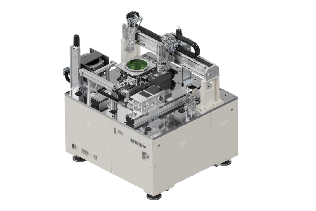
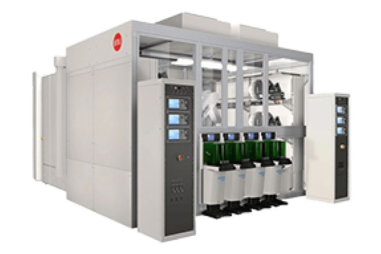
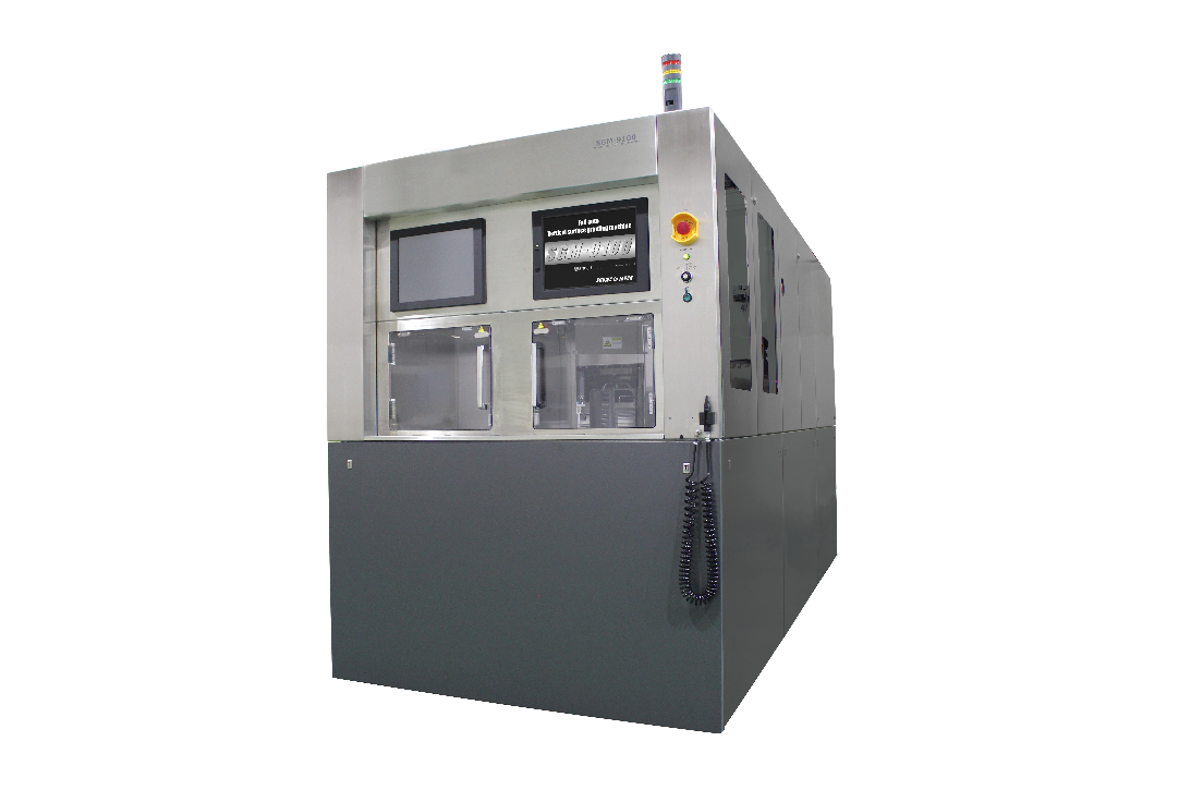
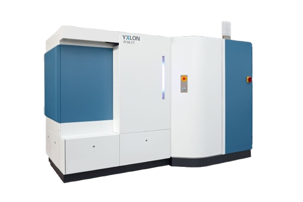
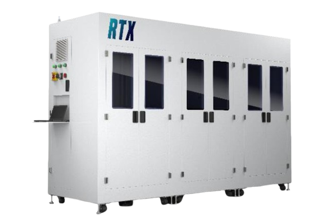
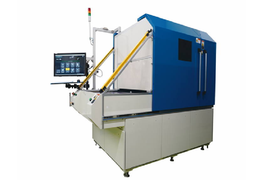
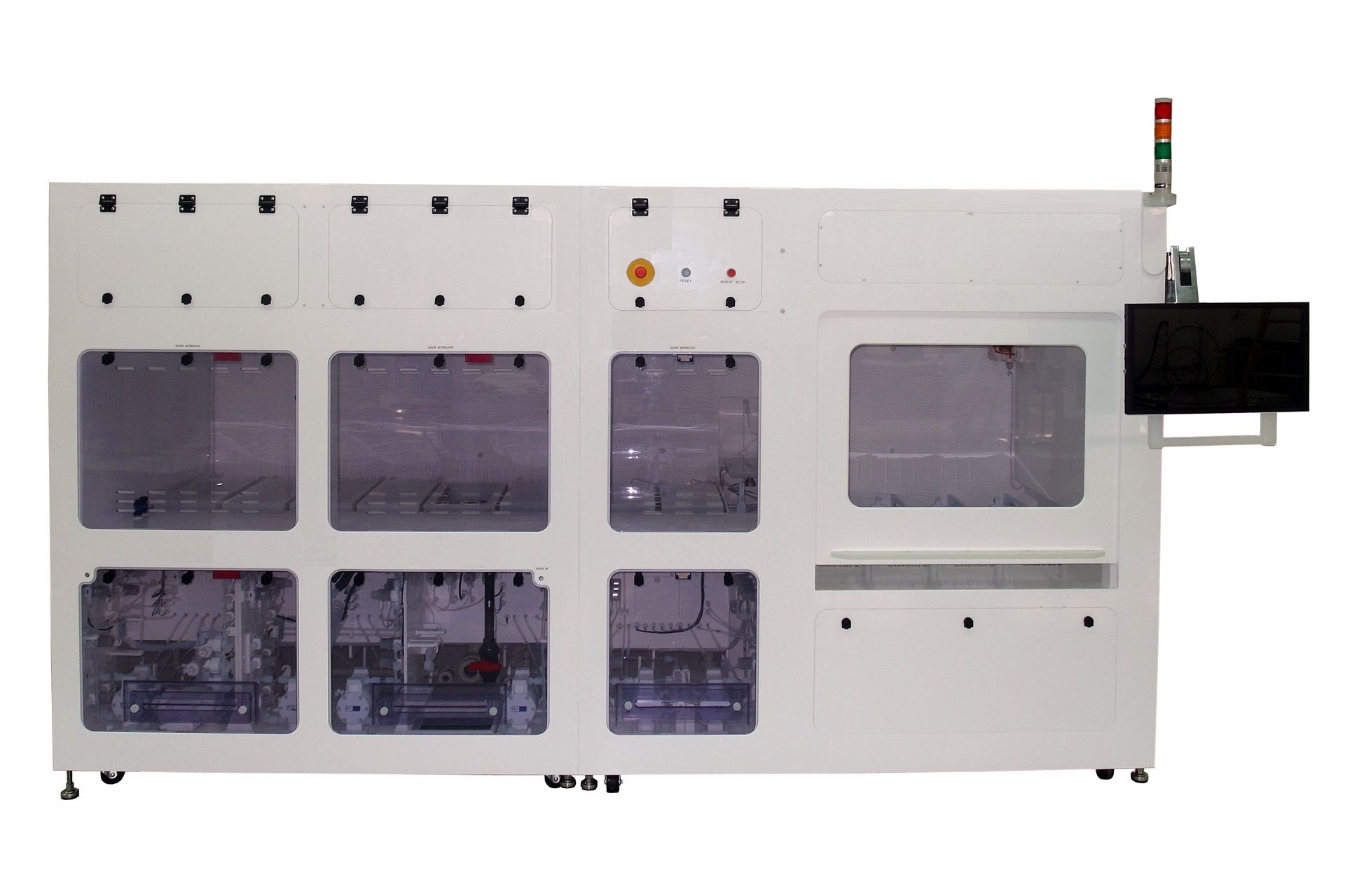
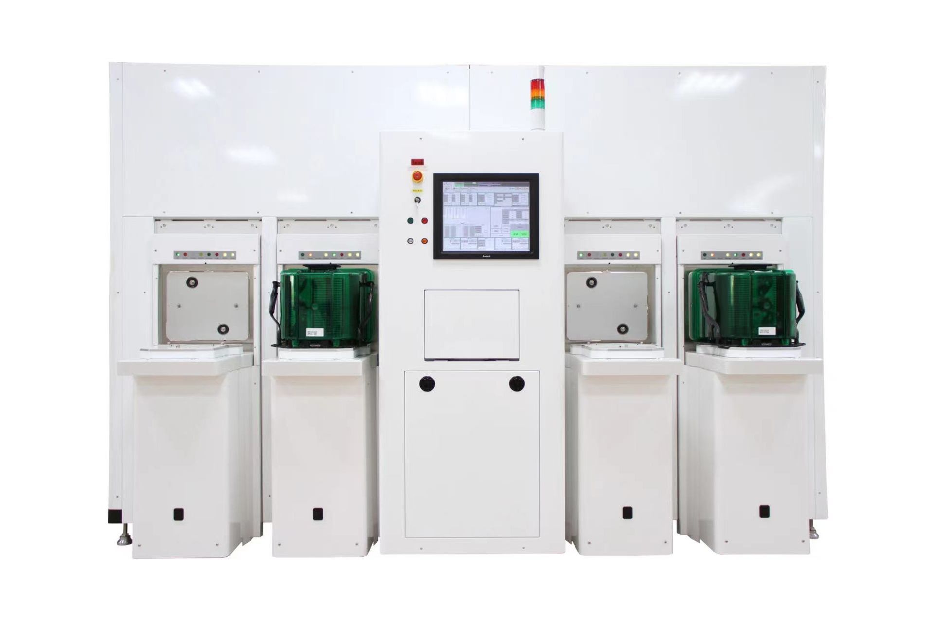
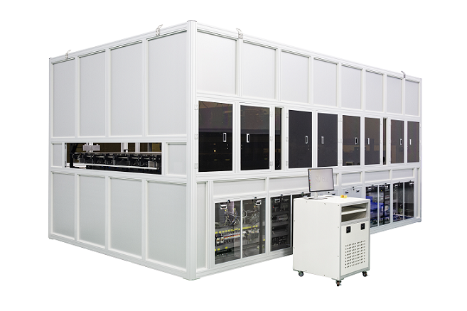
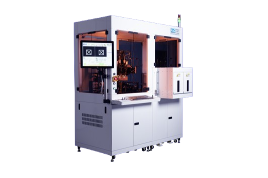
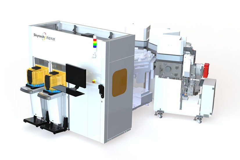
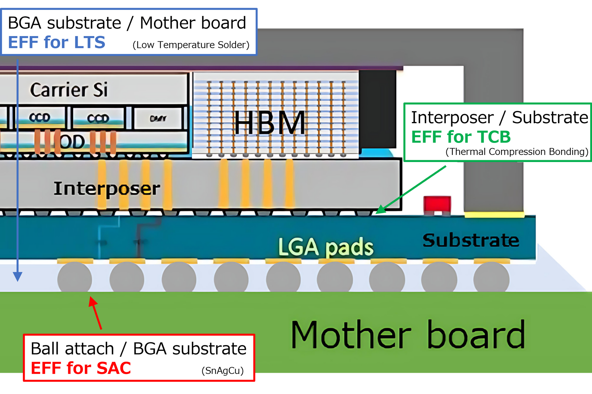
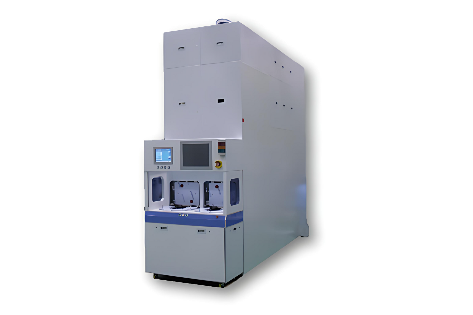
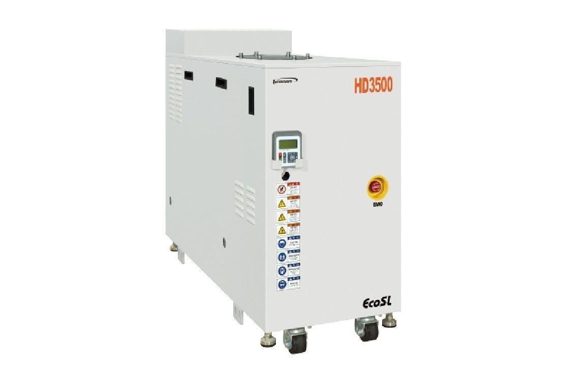
Six-sided inspection and transfer equipment
Taiwan Japanese Special Agents
Six-sided inspection and transfer equipment
Taiwan Japanese Special Agents
- 1. The number of nozzles can be changed to transfer chips of various sizes (up to 16 pieces)
- Use 3 types of cameras to perform 6-side inspection (top/back/side)
- The input and tray modes can be adjusted according to needs
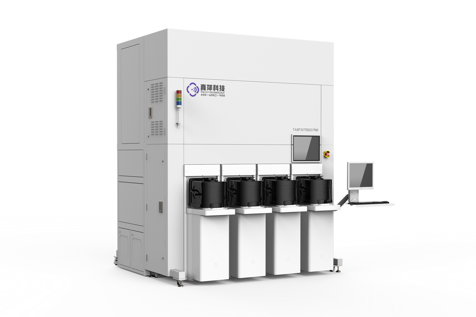
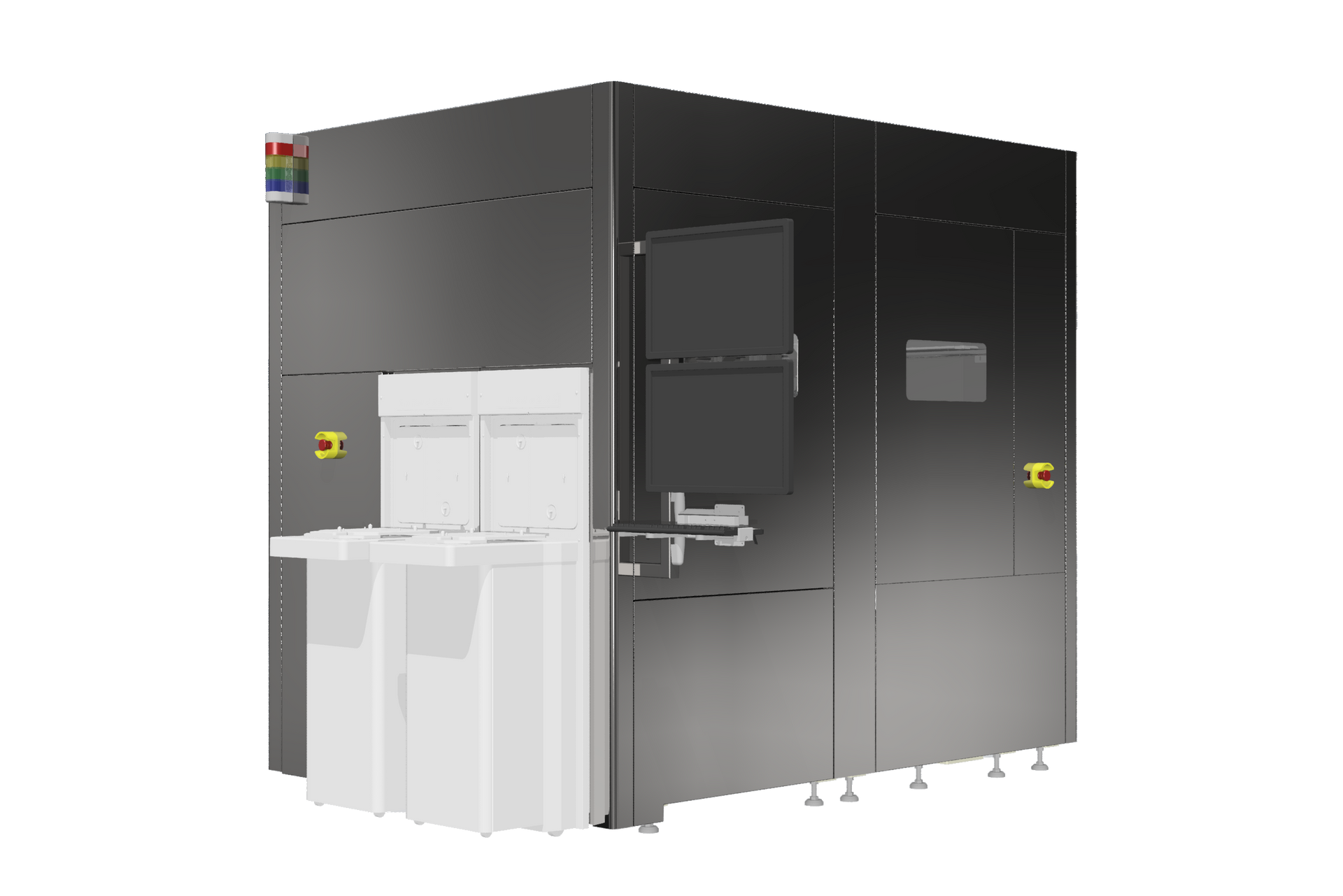
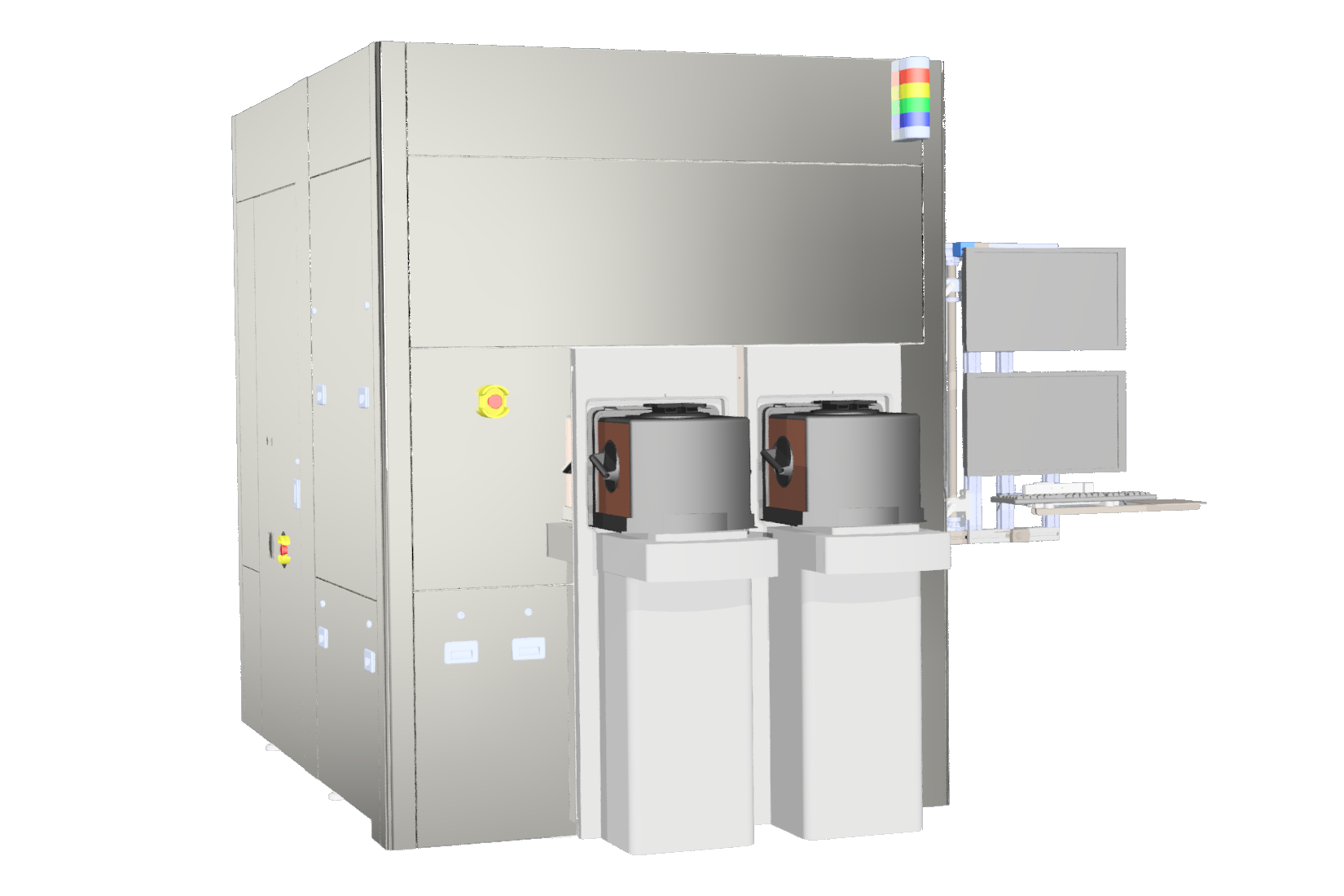
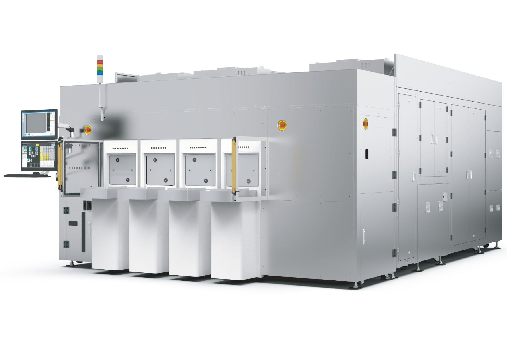
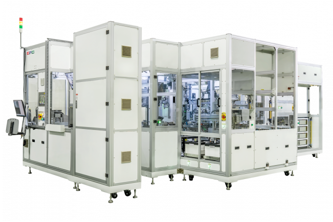
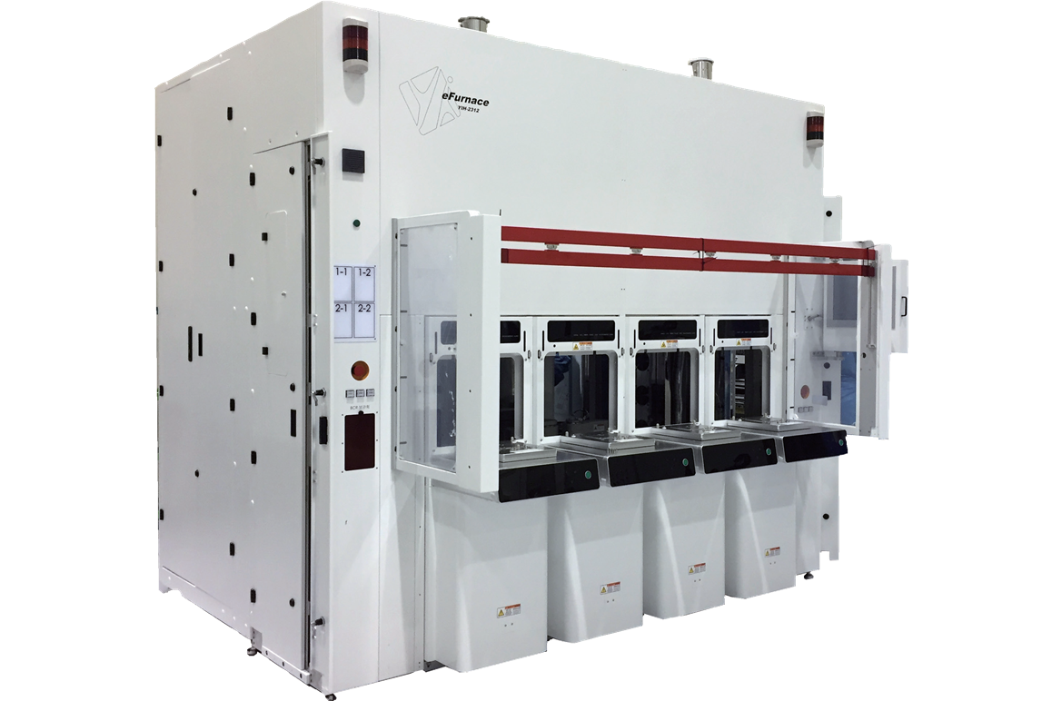
Fully automatic vertical tube furnace
Zhen Ping
Fully automatic vertical tube furnace
Zhen Ping
- Integrated human-machine operation system, continuous automated production, high work efficiency, saving labor costs, electricity and process time
- FEC heating, rapid heating and good uniformity
- High-quality stainless steel material, the surface is physically and chemically polished to ensure cleanliness
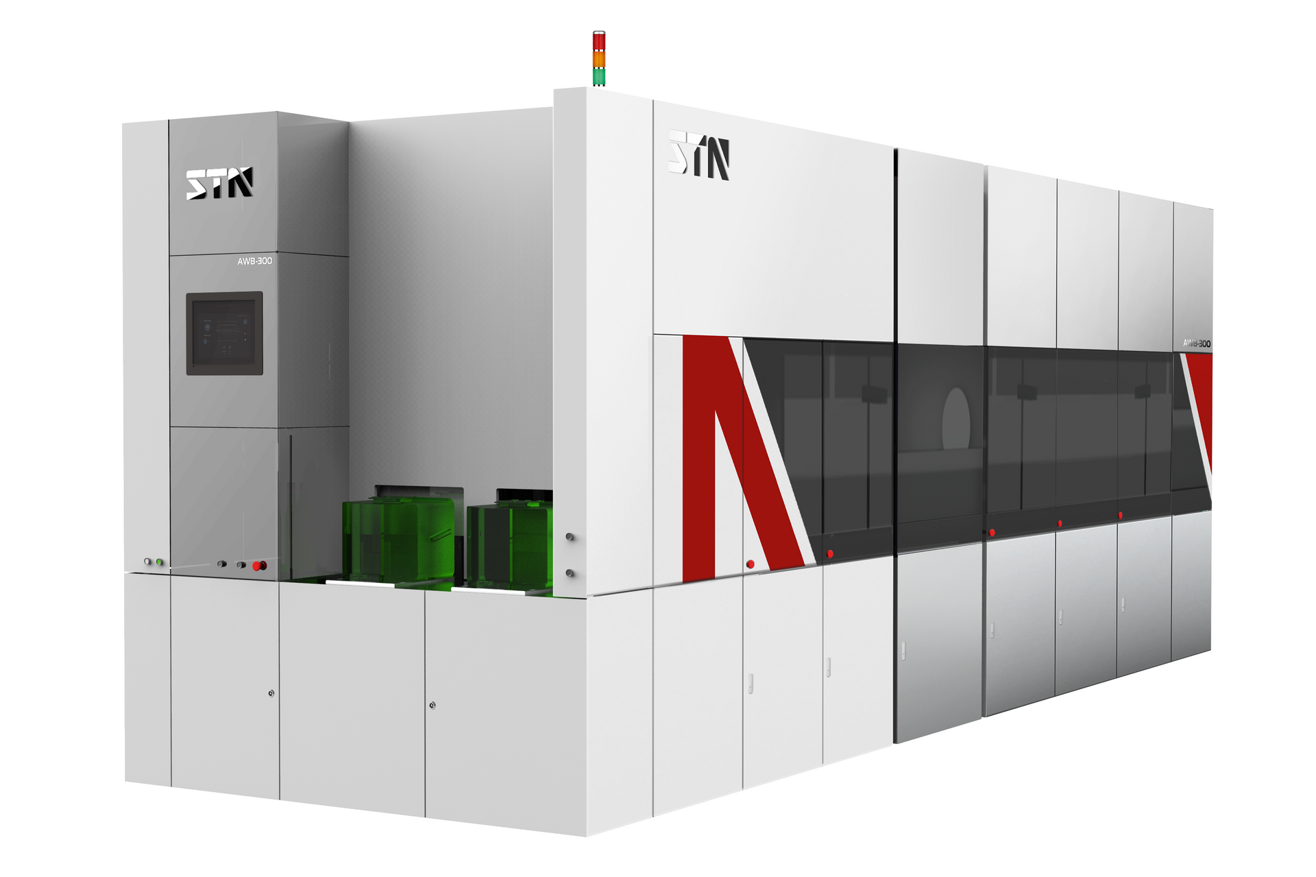
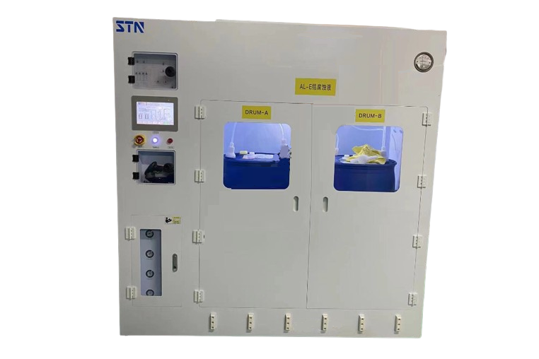
Recycling and reuse system
Ontario
Recycling and reuse system
Ontario
- Reduce CeO2 by 70% and recycle 60% of wastewater
- Automatic batch recycling production without changing parameters
- Same polishing yield as stock solution
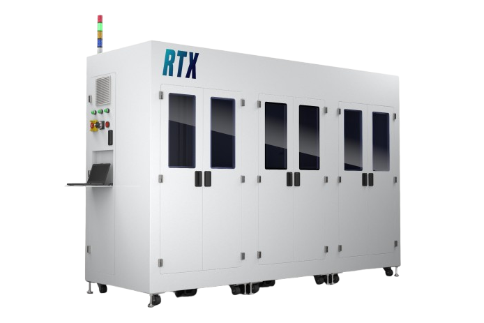
Horizontal furnace tube
BTU
Horizontal furnace tube
BTU
- 200mm and 300mm integrated fully automated conveying
- Each tube operates independently
- Slip free
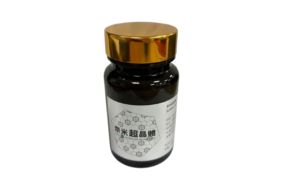
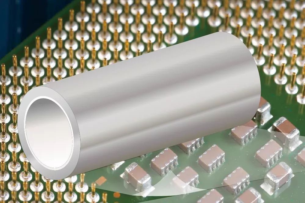
Conductive nano-supercrystals
Haosheng Technology
Conductive nano-supercrystals
Haosheng Technology
- Improve power quality and increase effective power
- Improve power generation capacity and reduce degradation rate
- ESG products are non-toxic, green energy and environmentally friendly
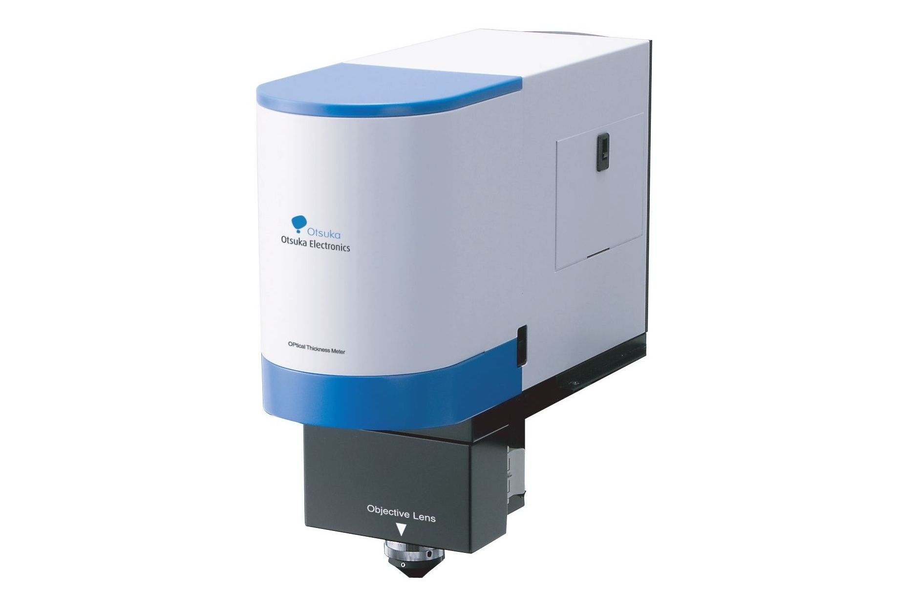
Fully automatic optical inspection equipment white light interferometer
Qinghe Optical
Fully automatic optical inspection equipment white light interferometer
Qinghe Optical
- Measure the dimensions of a specified location or pattern on a wafer/bare wafer after integrated circuit formation and dicing.
- Generate a 3D model based on the information obtained when measuring height, and use it as a simplified SEM function.
- Can also perform mixed measurements of line width (2D) x height (3D)
Defect IR inspection equipment
Qinghe Optical
Defect IR inspection equipment
Qinghe Optical
- We have extensive experience in various inspection projects such as power devices, CMOS, crystals (tuning forks), and inkjet heads.
- We can perform non-destructive precision measurement and inspection of the positional offset of the patterns on the front and back of wafers, and can also handle wafer surface-surface and wafer surface-interface (internal pattern) inspections.
- Equipped with a dedicated DSI optical engine for high-precision measurement; the repeatability of the measurement can reach 3σ≦0.2~0.02μm.
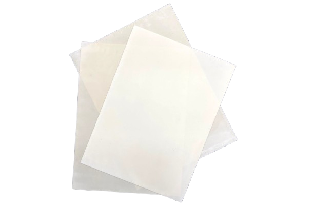
Silicon nitride substrate
Super Energy High-Tech
Silicon nitride substrate
Super Energy High-Tech
- High strength: resistant to pressure, folding and breaking, can achieve lighter and thinner components and improve heat dissipation efficiency
- High thermal conductivity, good heat dissipation effect, good insulation performance, no leakage risk
- Suitable for ultra-fast charging, new energy vehicles and various power components
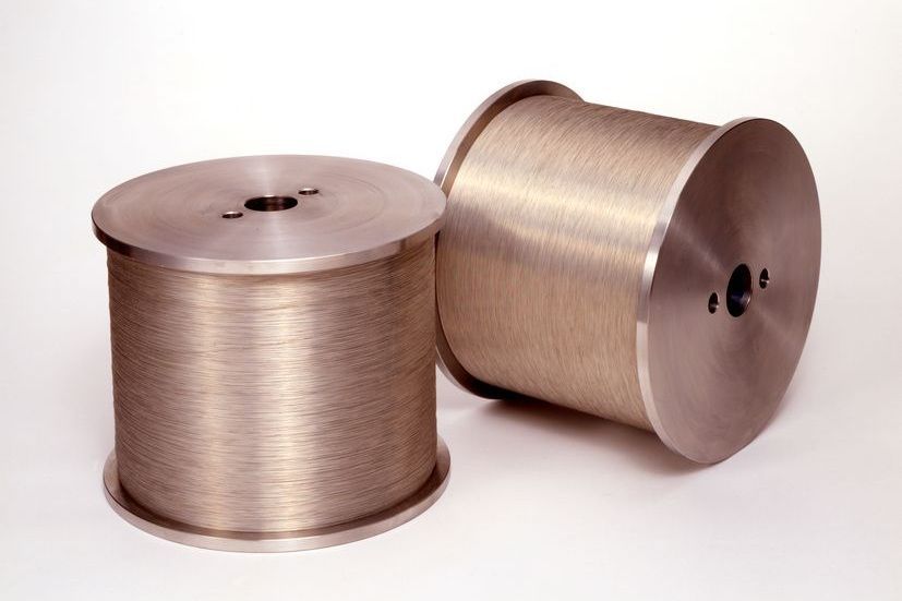
Diamond Line
ASAHI Diamond
Diamond Line
ASAHI Diamond
- Can shorten cutting time and reduce chip damage
- Thin the chip
- After cutting, the thickness of the chip remains the same
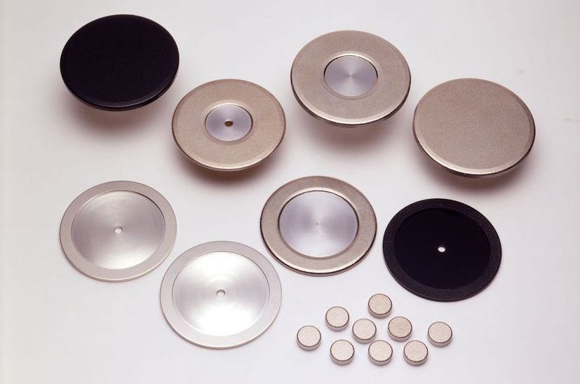
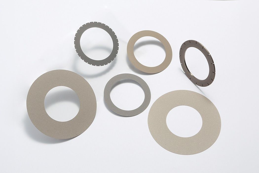
Notch Wafer Groove Grinding Wheel
ASAHI Diamond
Notch Wafer Groove Grinding Wheel
ASAHI Diamond
- Wafer chamfering
- Applicable to 2"~12" sizes
- Single groove and multi-groove types
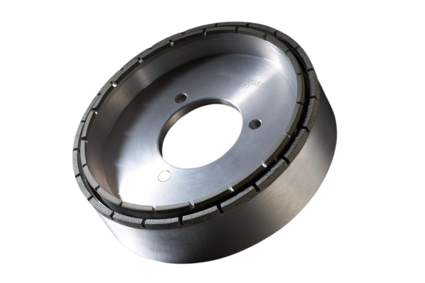
Double Disc Straight Groove Grinding (DDSG)
ASAHI Diamond
Double Disc Straight Groove Grinding (DDSG)
ASAHI Diamond
- Double-sided thinning grinding wheel
- Use ultra-fine abrasive grain to increase grinding force
- Grinding wheels of different specifications can be customized according to customer equipment requirements
Polishing pad dresser
ASAHI Diamond
Polishing pad dresser
ASAHI Diamond
- Improve polishing performance
- Reduce scratches on wafer surface
- Different types can be customized according to customer equipment requirements
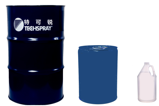
Precision V Coolant
ITW Techspray
Precision V Coolant
ITW Techspray
- Excellent heat transfer function and efficiency, good temperature regulation function
- High specific heat capacity, high dielectric strength, low dielectric constant
- Excellent chemical compatibility, high boiling point
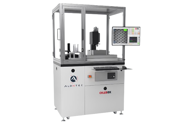
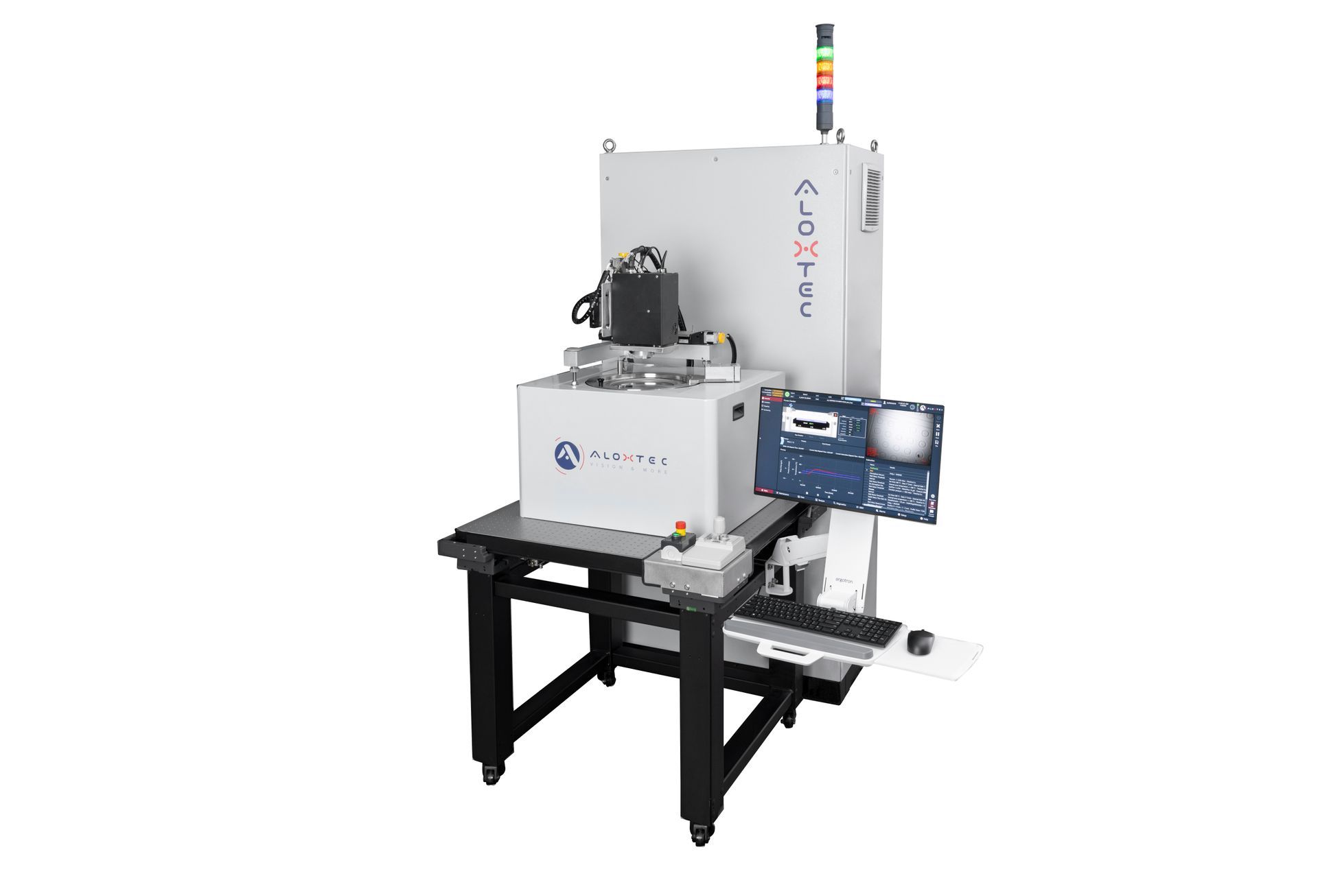
VCSEL oxidation aperture automatic measurement equipment
Aloxtec
VCSEL oxidation aperture automatic measurement equipment
Aloxtec
- Specially used for VCSEL aperture measurement
- Supports manual/automatic
- Can correspond to 20/50/100x CCD lens
Wafer wheel cutting cleaning agent
Nichiha Seiko
Wafer wheel cutting cleaning agent
Nichiha Seiko
- Extremely high lubricity can reduce cutting resistance and the possibility of fragmentation during wheel cutting.
- Applicable to CIS sensor packaging, MEMS packaging, fan-out packaging and other industries.
- Can improve cutting efficiency, good protection effect, significantly reduce splinters, easy to clean.
Grinding and thinning machine
Hidekazu
Grinding and thinning machine
Hidekazu
- Compatible with 4-inch, 6-inch, and 8-inch SiC thinning machines
- Can thin 150/150mm bonded wafers of the same size
- Provides non-contact thinning real-time monitoring
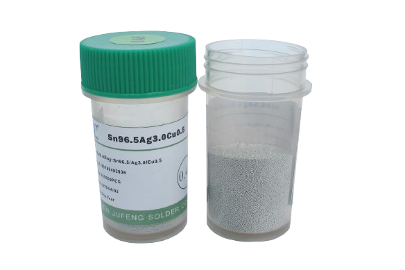
soldering lugs
Jufeng
soldering lugs
Jufeng
- High stability and high reliability
- Excellent electrical and thermal conductivity
- High strength and good fatigue resistance

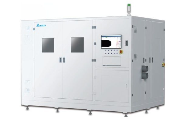
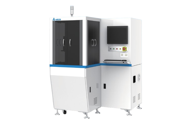
Fully automatic wafer hole inspection machine
Delta
Fully automatic wafer hole inspection machine
Delta
- Defect detection system - resolution: 1.7um; hole inspection depth inspection
- AOI AI screening function to prevent dirty particles from being screened
Wafer edge grinding machine
Delta
Wafer edge grinding machine
Delta
- Improve wafer process efficiency and shorten production cycle
- Improve the stability of subsequent processes
- Automation function can automatically adjust parameters and perform processing, reducing the need for manual work
AOI appearance inspection and sorting machine
Delta
AOI appearance inspection and sorting machine
Delta
- Comprehensive inspection, AOI AI intelligent inspection algorithm, supplemented by all-round light and dark three-field optical imaging
- One machine with multiple functions, integrating resistance, flatness, and inspection modules
- Flexible production: fast size switching, automatic line change
- The degree of automation can be freely matched with various defect detection according to customer requirements, while achieving automation
Microspectroscopy film thickness meter
Otsuka
Microspectroscopy film thickness meter
Otsuka
- High-precision absolute reflectivity measurement (multi-layer film thickness, optical constants) using microspectroscopy
- High-speed measurement in 1.1 seconds
- Equipped with marco function, various measurement conditions can be customized
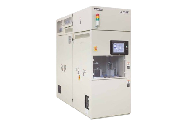
Atmospheric pressure CVD
Amaya
Atmospheric pressure CVD
Amaya
- New monolithic atmospheric pressure CVD for hard mask and ILD oxide insulating layer
- New monolithic design can cope with warping of third generation semiconductor SiC wafers
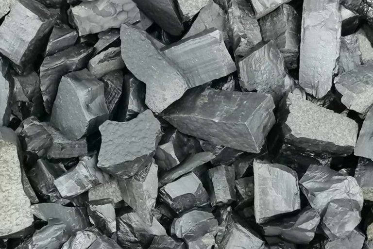
Silicon carbide powder
Guanlan New Materials
Silicon carbide powder
Guanlan New Materials
- High-purity CVD silicon carbide crystal growth raw material
- Large particle size, faster, thicker, and higher purity crystal growth
- Low crystal growth cost
X-ray Ingot Inspection Equipment
Ruisheng Optoelectronics
X-ray Ingot Inspection Equipment
Ruisheng Optoelectronics
- Avoids waste of resources and increased production costs
- Effectively ensures product quality and safety, and can detect potential problems in advance
- Equipped with advanced image processing and analysis software to automatically identify and classify different types of defects
Wafer box automatic packaging machine
Yifa Precision Machine
Wafer box automatic packaging machine
Yifa Precision Machine
- Replace manual labor, maintain consistent product quality, and effectively reduce the risk of wafer breakage.
- Automatic vacuum sealing ensures that the FOUP will not be damaged. Monitoring systems are installed at key sites to keep records and avoid losses caused by customer complaints.
- E84 communication, compatible with the OHT overhead crane system and the MR system's automated loading function, can be put into large-scale production.
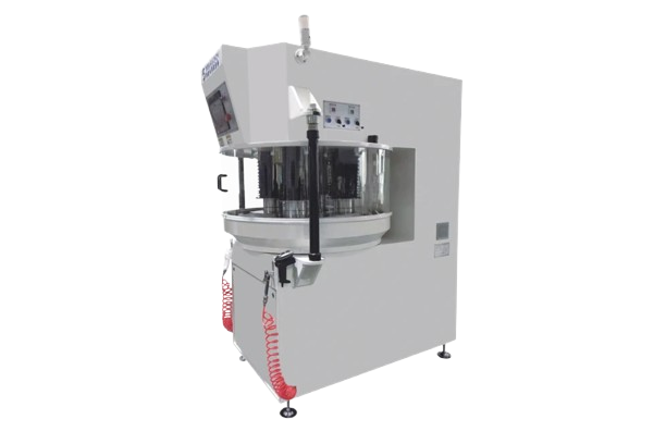
CMP polishing machine
Mengqi Semiconductor
CMP polishing machine
Mengqi Semiconductor
- Using PLC touch screen control system, equipment parameter setting and operation are simple and convenient, and the system operation stability is high.
- Using cylinder pressurization method, closed-loop control of pressure is achieved through electric proportional valve control to ensure extremely high pressure accuracy and stability.
- The polishing plate and upper pressure plate are equipped with water cooling function to ensure high efficiency of polishing liquid while reducing deformation of the polishing plate surface.
Kalrez perfluoroelastomer seal
DuPont
Kalrez perfluoroelastomer seal
DuPont
- Chemical resistance, showing excellent stability under most chemicals
- Heat resistance of nearly 300 degrees Celsius, still able to maintain the physical properties of rubber at high temperatures
- Extend the seal life and average maintenance interval time, and improve the yield rate of semiconductor products
Polishing wastewater recovery system
Inlite
Polishing wastewater recovery system
Inlite
- Use patented technology to recycle and replace 70% of grinding powder/polishing powder
- Recycle 60% of water resources
- Environmentally friendly and save raw material costs
UV Cutting Tape
Good Plus
UV Cutting Tape
Good Plus
- After irradiation with ultraviolet rays of a specific wavelength, the adhesion is reduced to an extremely low level, making it easy to remove the adhesive and film from the adhered object, making it easier to process.
- Suitable for wafer grinding, cutting processes, and cutting and transferring of various substrates or semiconductor electronics industries
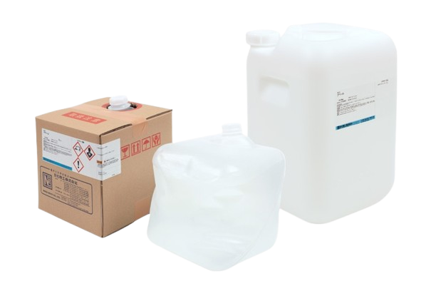
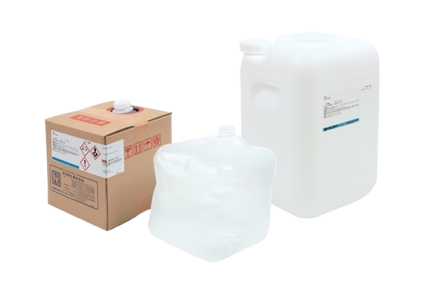
Drynon C moisturizer
Nichiha Seiko
Drynon C moisturizer
Nichiha Seiko
- Surfactants used after final polishing of silicon wafers and glass materials can effectively inhibit particles, HAZE and prevent metal contamination
Kilalaclean Wax Remover
Nichiha Seiko
Kilalaclean Wax Remover
Nichiha Seiko
- Suitable for high-purity cleaning of various semiconductor materials after polishing and cleaning of liquid/solid wax produced by Nichika Seiko
- Suitable for precision cleaning of equipment, abrasives and equipment parts that come into contact with wafers
- Low erosion rate, can be diluted with pure water, safer and more economical
Devel Ceramic Dish Cleaner
Nichiha Seiko
Devel Ceramic Dish Cleaner
Nichiha Seiko
- Inorganic cleaning agent, good for degreasing, suitable for wax removal and cleaning, with excellent effect
- Does not contain organic solvents, suitable for cleaning quartz, crystal, ceramics and other materials
- Safe and economical
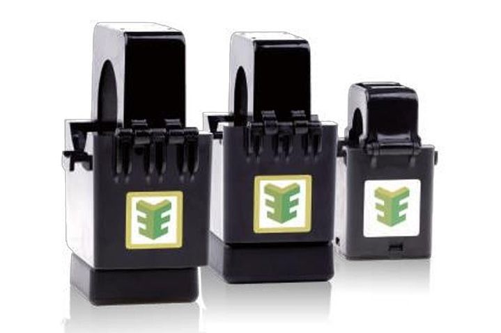
Smart Clamp Meter
3Egreen
Smart Clamp Meter
3Egreen
- Completely wireless clamp meter with self-charging, no wiring required
- Real-time power consumption monitoring with equipment anomaly alerts
- Quick installation without shutdown, avoiding production downtime, with low implementation cost
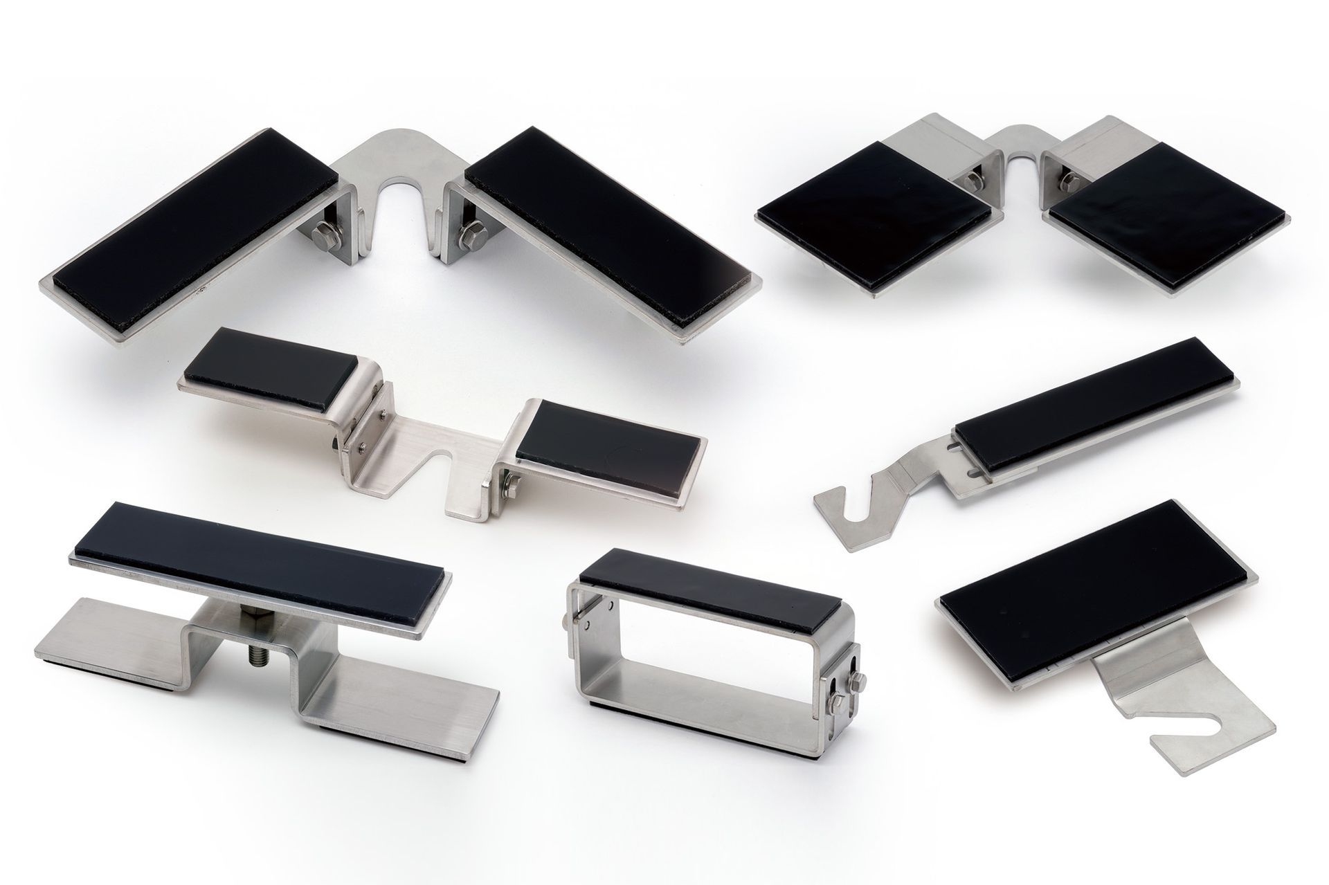
Vibration-Resistant Metal Base Foot
TAIWAN NITTOKU
Vibration-Resistant Metal Base Foot
TAIWAN NITTOKU
- Seismic resistance up to magnitude 7, supporting equipment weights up to 4 tons
- Easy installation and reconfiguration, washable and reusable
- Floor-friendly alternative to traditional rivet fixing, suitable for cleanroom environments
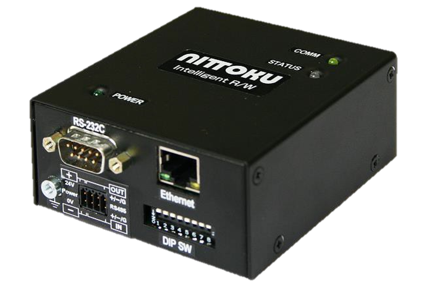
Low-Frequency RF ID Reader/Writer
TAIWAN NITTOKU
Low-Frequency RF ID Reader/Writer
TAIWAN NITTOKU
- Smallest footprint in the industry, supporting multiple communication interfaces
- Outstanding communication performance even in environments with electromagnetic noise and metal interference
- Supports semiconductor industry SEMI standards (SECS-GEM)
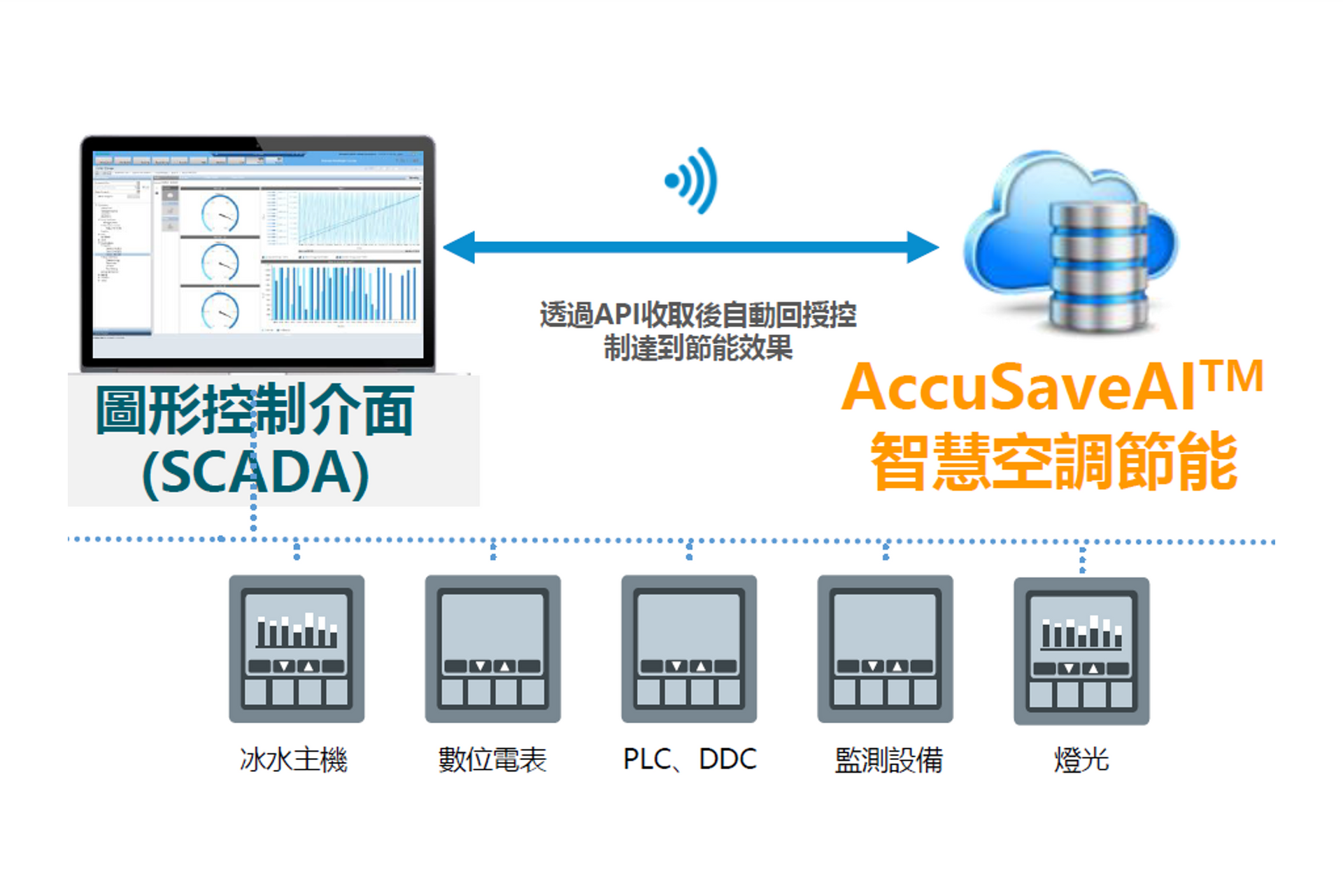
AccuSave AI Chiller Energy Saving System
ECOFIRST
AccuSave AI Chiller Energy Saving System
ECOFIRST
- Energy savings of 15% to 65%
- Improves air conditioning system efficiency
- Reduces operating costs
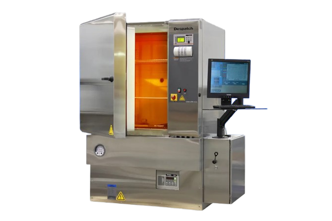
Oven
Despatch
Oven
Despatch
- With over a century of history, specializing in heat treatment oven technology
- Offering a full range from benchtop and cabinet ovens to ultra-large ovens, meeting the needs of various industries
Thin Wafer Dicing Blade
ASAHI Diamond
Thin Wafer Dicing Blade
ASAHI Diamond
- Widely used in various packages such as glass, ceramics, and compound materials
- Customizable bonding agents to suit both high rigidity and high cutting force requirements
- Available in three types: resin blades, metal blades, and electroformed blades
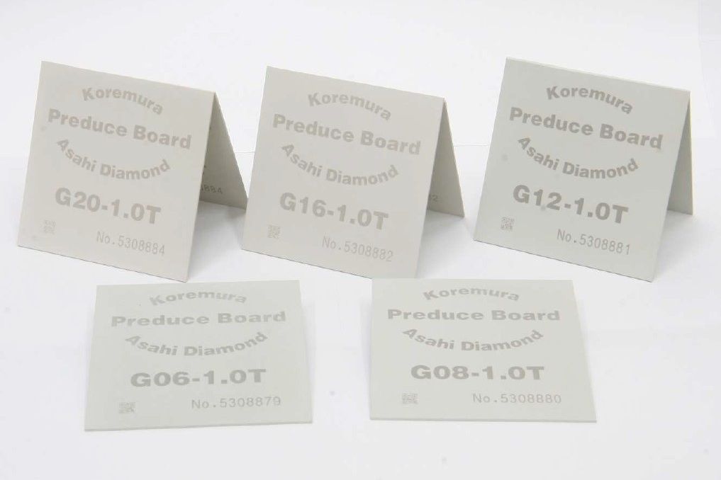
Dressing Board for Dicing Blades
ASAHI Diamond
Dressing Board for Dicing Blades
ASAHI Diamond
- Suitable for wafer dicing blades
- Improves cutting efficiency and reduces time costs
- Reduces coolant consumption
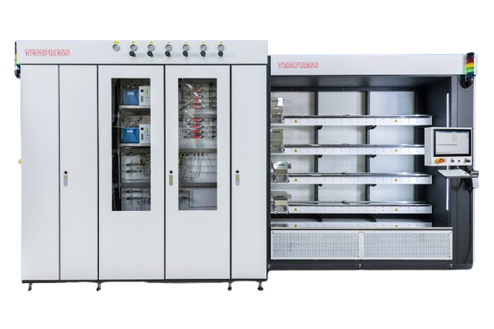
Horizontal Furnace
TEMPRESS
Horizontal Furnace
TEMPRESS
- Provides versatile atmospheric and CVD process chambers, suitable for any type of silicon wafer
- Capable of batch processing 25–200 wafers per tube
- Fully automated vertical and horizontal furnaces for high-temperature oxidation and LPCVD applications
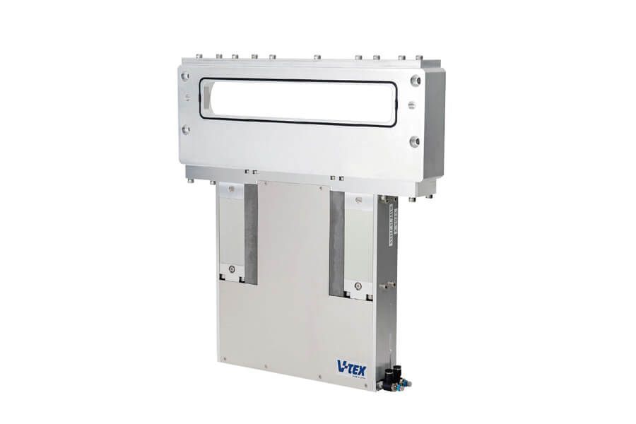
Process Chamber Gate Valve
V-TEX
Process Chamber Gate Valve
V-TEX
- No metal-to-metal friction inside the vacuum
- Streamlined design to reduce cost and space requirements
- Standard design supports 1 million cycles, featuring high durability and low maintenance
Wafer Surface Inspection System
TAKANO
Wafer Surface Inspection System
TAKANO
- High-speed color/monochrome inspection for wafer defects
- Optional ring illumination and transmitted illumination, each compatible with color filter sets
- Enhanced defect detection capability & productivity
Wafer Surface Particle Scanning Equipment
TAKANO
Wafer Surface Particle Scanning Equipment
TAKANO
- Capable of detecting wafer surface particles or defects
- Utilizes a violet-LD surface analyzer to effectively reduce operating costs
- High performance, high quality, and high measurement speed with easy operation
ALTEX Bump Height Measurement Equipment
TAKANO
ALTEX Bump Height Measurement Equipment
TAKANO
- High-precision bump height and coplanarity measurement with 3σ ≤ 1.0 μm
- Inspection time per sample is less than 2 seconds. With proprietary processing algorithms and dedicated hardware, tens of thousands of high-density bumps can be measured in an extremely short time
- Capable of measuring circular bumps as small as φ30 μm
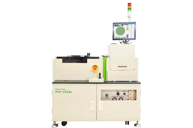
Circuit Probing Equipment
Plum Five
Circuit Probing Equipment
Plum Five
- Capable of probing standard wafers, thinned wafers, diced wafers, and substrates with special shapes
- Automatically transported from carriers via a controlled transfer system for subsequent inspection
- Supports multi-zone measurement
Double-Sided Lithography Inspection System
SEIWA Optical
Double-Sided Lithography Inspection System
SEIWA Optical
- Wide range of applications, including exposure offset inspection, defect inspection, and CoWoS HBM offset inspection
- Top-side alignment and back-side alignment processes
- 3D inspection technologies such as white light interferometry, confocal microscopy, and AFM
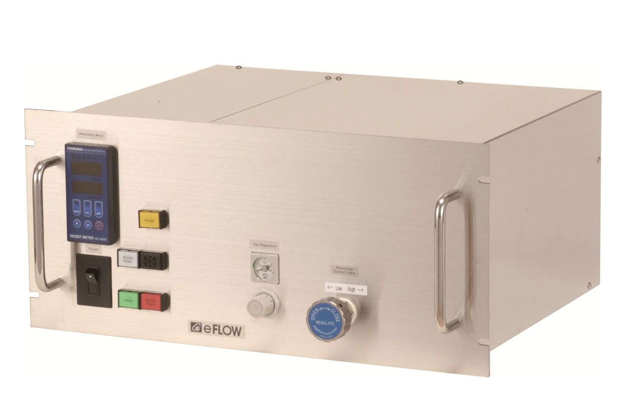
eFLOW Anti-Static System for Ultrapure Water
DIC
eFLOW Anti-Static System for Ultrapure Water
DIC
- Simple structure with low failure rate
- Unique piping distribution design for easy resistivity control and excellent stability
- Long service life of the CO₂ supply module
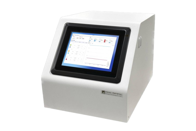
Real-time Chemical Concentration Analyzer (Drug withdrawal cycle type)
Mega Crystal
Real-time Chemical Concentration Analyzer (Drug withdrawal cycle type)
Mega Crystal
- High Accuracy: Capable of detecting trace additives and metal ions (Au, Cu, Pd, Si, Ni, etc.) down to below 100 ppm
- Versatile Analysis: Suitable for mixed chemical solutions, capable of analyzing 6 to 8 components simultaneously
- Rapid Detection: No consumables required, analysis results in as fast as 10 seconds
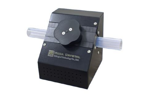
Real-time Chemical Concentration Analyzer (Clip type)
Mega Crystal
Real-time Chemical Concentration Analyzer (Clip type)
Mega Crystal
- Non-contact Detection: No direct contact with chemical solutions, preventing contamination and loss
- High Temperature Tolerance: Capable of analyzing chemical solutions up to 160°C
- Flexible Usage: Wide concentration range supported, no hardware modification required for concentration changes
Wafer Cleaner
LJH
Wafer Cleaner
LJH
- Chemical supply system, wet bench and single-wafer cleaning machine
- Professional facility engineering services
Equipment Performance and Failure Prevention Quick Screening Kit
SmartTag
Equipment Performance and Failure Prevention Quick Screening Kit
SmartTag
- Real-time monitoring and measurement of specific parameters such as vibration, temperature, and humidity
- Equipped with wireless transmission, allowing alert thresholds to be set and notifications to be sent
- AIoT edge computing device with a built-in data compression algorithm (Decay Rate)
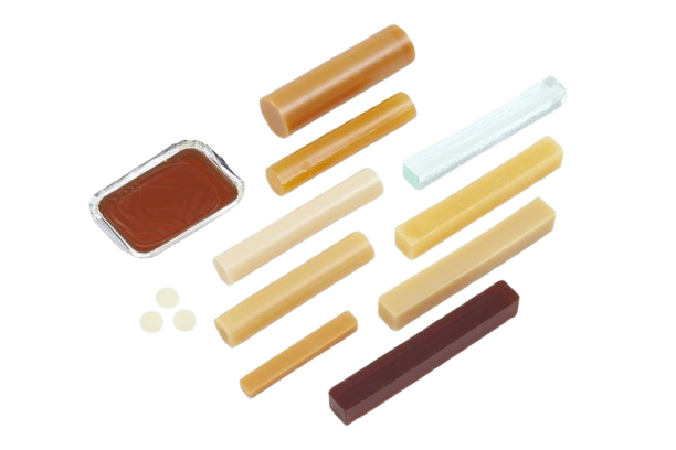
Solid Wax for Wafer Slicing and Grinding
NIKKA SEIKO
Solid Wax for Wafer Slicing and Grinding
NIKKA SEIKO
- High-strength temporary bonding wax, with customizable strength requirements based on different materials and processes
- Easy to operate, with product options available based on operating temperature, working viscosity, and heat resistance
- Easy to clean, with tailored cleaning solutions available to meet customer needs, leaving no residual contamination
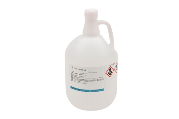
Wafer Laser Dicing Protective Coating Chemical
NIKKA SEIKO
Wafer Laser Dicing Protective Coating Chemical
NIKKA SEIKO
- Water-soluble protective solution that prevents laser-cutting byproducts from directly contacting or reattaching to the wafer
- Applicable to industries such as fan-out packaging, CIS sensor packaging, DDIC chip COG/COF packaging, and memory chip bumping packaging
- Excellent protection, easy to clean, and stable performance
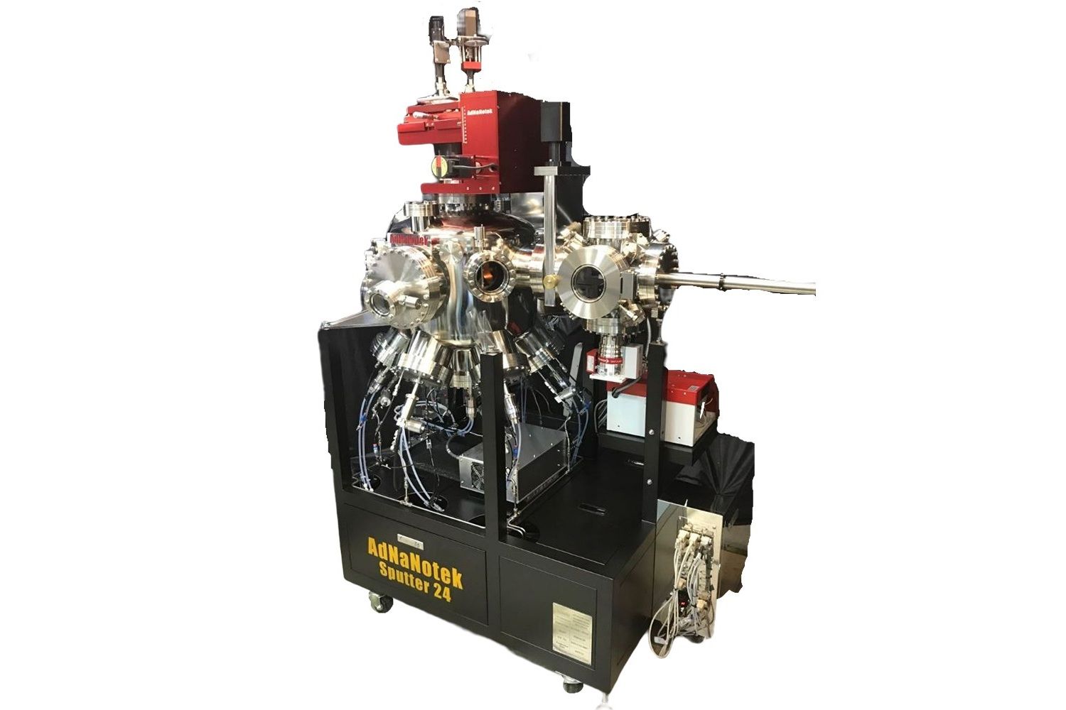
Ion Beam Etching (IBE) Tool
Adnano
Ion Beam Etching (IBE) Tool
Adnano
- Ion source low-temperature etching
- Ion source physical vapor deposition (PVD)
- Dry etching
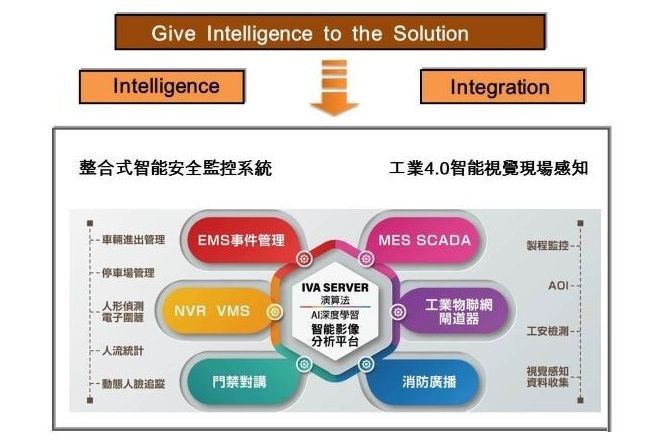
Factory Vision Automation System
TDV
Factory Vision Automation System
TDV
- Software developer and system integrator for front-end and back-end of Industrial IoT
- Security industry
- Intelligent transportation systems (ITS), Industry 4.0 applications, Smart City, and material handling/warehousing
Single-Wafer Wet Process Equipment
Cisom
Single-Wafer Wet Process Equipment
Cisom
- Short single-wafer processing time with high efficiency
- Strong particle removal capability, low breakage rate, and high reliability
- Reduced sulfuric acid consumption with enhanced cleaning performance, effectively lowering cleaning costs
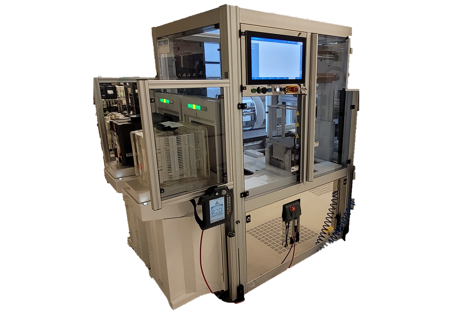
SOI Wafer Smart Cut™ Technology Splitting Equipment
R2D Automation
SOI Wafer Smart Cut™ Technology Splitting Equipment
R2D Automation
- The world’s leading manufacturer of Smart Cut technology splitting equipment for SOI wafers
- Provides stand-alone systems or fully automated Smart Cut wafer splitting equipment integrated with horizontal/vertical furnaces
High-Temperature Wet Oxidation Furnace
Aloxtec
High-Temperature Wet Oxidation Furnace
Aloxtec
- Moisture oxidation of III-V compound semiconductor materials
- Moisture oxidation of VCSEL devices
- Moisture oxidation of AlGaAs DBR LED devices
Resin Type Ingot Slicing Beam
DWi DOW INNOVATION
Resin Type Ingot Slicing Beam
DWi DOW INNOVATION
- Used in band saw and wire saw processes for silicon ingot slicing, improving production quality
- Customizable in different sizes according to customer requirements
- Easily compatible with adhesive products, enhancing production efficiency

Soda Lime Glass
NSG
Soda Lime Glass
NSG
- Applied in TN-LCD, STN-LCD products
- Main glass material used in touch panels
- Can be used as the main material of the protective layer glass on the upper layer of the touch panel
- Ultra-thin alkali glass
- Global flat glass market share is 50%
- Glass thickness: 0.28t~1.1t
- Maximum motherboard glass size: G6
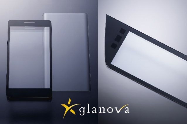
Glanova
NSG
Glanova
NSG
- Glanova for smartphone
- Chemically strengthened thin glass for Automotive applications
- High and sufficient strength
- Easy heat 3D forming by its low softening point
- Lower cost than other competitive materials
Panel-Level Automatic Optical Inspection Tool (AOIL)
3i system
Panel-Level Automatic Optical Inspection Tool (AOIL)
3i system
- High-speed focusing microscope system with transmission and reflection modes
- Efficient image processing and intelligent algorithms, magnification up to 100 times
- Full-area measurement, no non-inspection area
Panel-Level Automatic Optical Inspection Tool (AOIH)
3i system
Panel-Level Automatic Optical Inspection Tool (AOIH)
3i system
- Applicable to defect detection of various panels such as array, color film, touch screen and organic light-emitting diode
- Maximum measurement accuracy is 1.0 micron
- Maximum detection speed can be customized
CDOL
3i system
CDOL
3i system
- High-speed focusing microscope system with transmission and reflection modes
- Efficient image processing and intelligent algorithms, magnification up to 100 times
- Full-area measurement, no non-inspection area
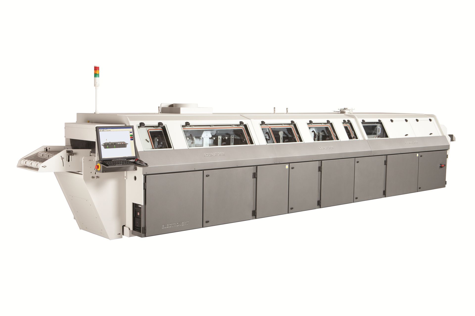
Electrovert Cleaner
ITW EAE
Electrovert Cleaner
ITW EAE
- All-round spray pattern improves cleaning under low-distance components and eliminates shadow effects
- Adopts mixed spray technology
- Provides a variety of integrated design functions to save chemicals and electricity and reduce consumption
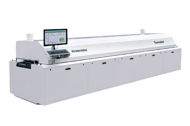
Centurion™ Reflow
ITW EAE
Centurion™ Reflow
ITW EAE
- With strict closed-loop process control, it is designed for today's high-throughput assembly environment
- It significantly reduces the thermal difference of the product and uses less energy
- It reduces maintenance requirements and lowers the cost of ownership through cutting-edge flux processing technology
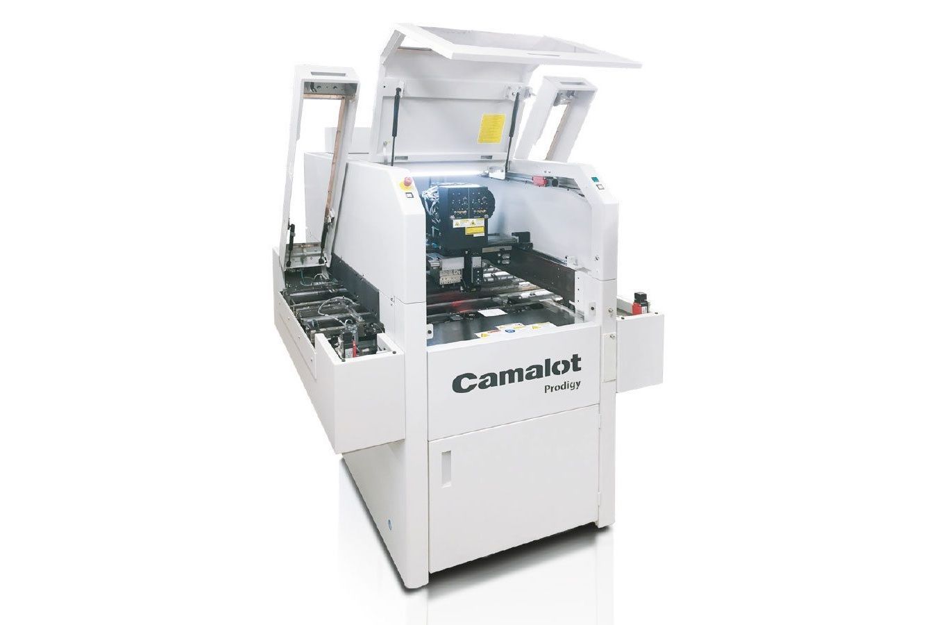
Prodigy™ Dispenser
ITW EAE
Prodigy™ Dispenser
ITW EAE
- ± 35μ 3 Sigma dispensing accuracy at full speed
- Innovative board grading options that expand the dispensing area in the X direction by 1-3 times, with a maximum processing size of 900 mm
- Patented tilt and rotation technology that reduces KOZ and improves capillary flow of bottom fill
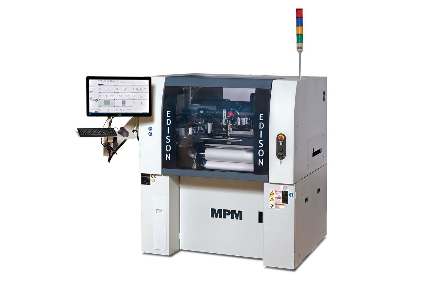
Edison™ Printer
ITW EAE
Edison™ Printer
ITW EAE
- An optimized system processing speed can increase the margin of key printing parameters
- Wet printing accuracy improved by 25%: built-in ±8 micron alignment accuracy and ±15 micron printing repeatability (≥2 Cpk @ 6σ)
- No printing deviation: high-precision pressure sensor can eliminate pressure changes before and after, keeping the pressure of the entire surface constant
High-Resolution Mask Aligner/Exposure Tool
NXQ
High-Resolution Mask Aligner/Exposure Tool
NXQ
High-Resolution Semi-Automatic and Automatic Mask Aligner/Exposure Systems for LED, Compound Semiconductor, and Advanced Packaging Applications
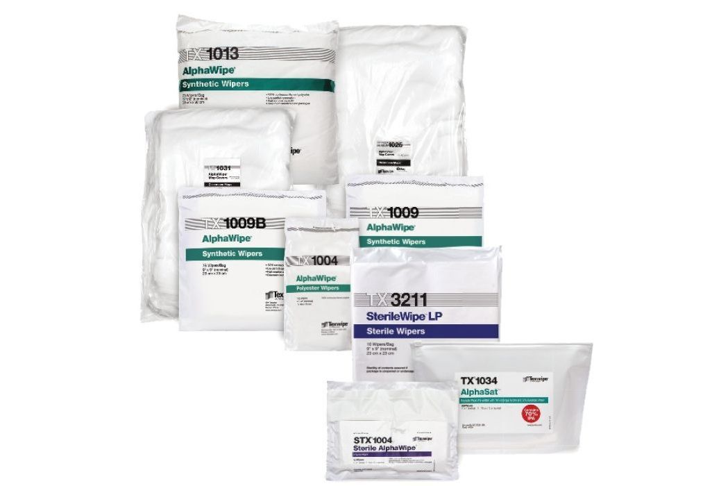
Cleanroom Wipers
Texwipe
Cleanroom Wipers
Texwipe
- Ensure the wafer surface is clean and dust-free, which helps to ensure process stability and product quality
- Anti-static ability helps to protect the safety of wafers and processes
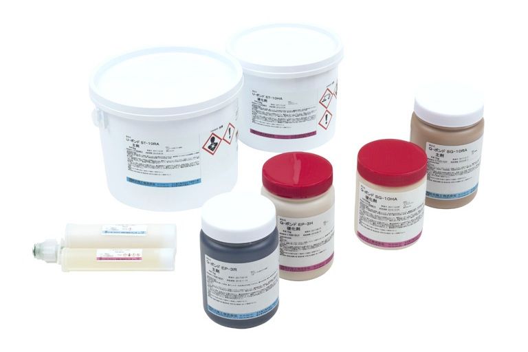
Adhesive for Bonding Ingot to Beam Prior to Slicing
NIKKA SEIKO
Adhesive for Bonding Ingot to Beam Prior to Slicing
NIKKA SEIKO
- Temporary adhesive specially developed for silicon ingot slicing processes (not for permanent fixing or packaging)
- Two-component epoxy resin used to bond workpieces to resin beams (slicing beams) or support carriers
- High adhesion strength, high hardness, and peelable
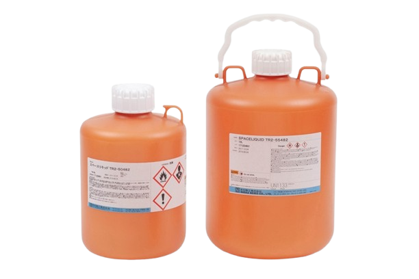
Liquid Wax for Wafer Temporary Wafer Bonding
NIKKA SEIKO
Liquid Wax for Wafer Temporary Wafer Bonding
NIKKA SEIKO
- Applicable to processes such as thin wafer backside processing, deep silicon etching, and TSV via formation
- Suitable for wafer-level packaging, compound semiconductors, and MEMS industries
- High temperature resistance, chemical corrosion resistance, easy to clean, and stable performance
Wet Bench
STN
Wet Bench
STN
- Customizable design and production
- Mostly adopts an integrated non-jointed design, which is not easy to produce particles and leakage, and has low maintenance costs
- Can be used for wafer cleaning to remove surface dust particles, etching, and photoresist removal
CDU
STN
CDU
STN
- 1. Imported materials and integrated non-jointed design are used , which is not easy to cause liquid leakage and has low maintenance costs
- 2. Customizable
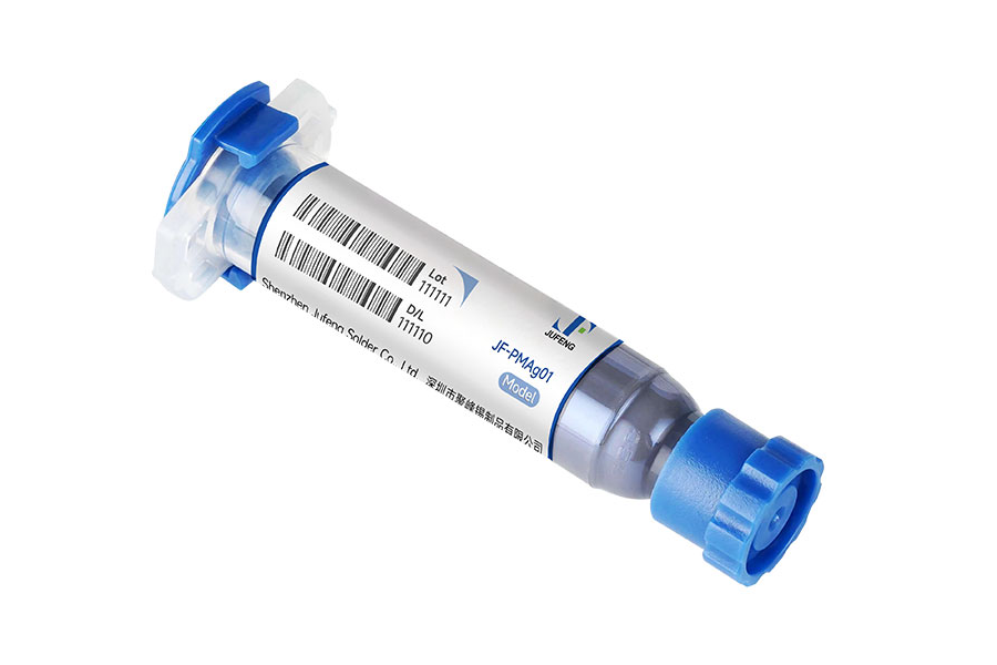
Sintered Silver Paste
JuFeng
Sintered Silver Paste
JuFeng
- High-power electronic component packaging material, using advanced nano silver technology
- Can be sintered and applied directly on copper plates without gold or silver plating
- Provide dispensing, screen printing, pressureless, and pressure sintering
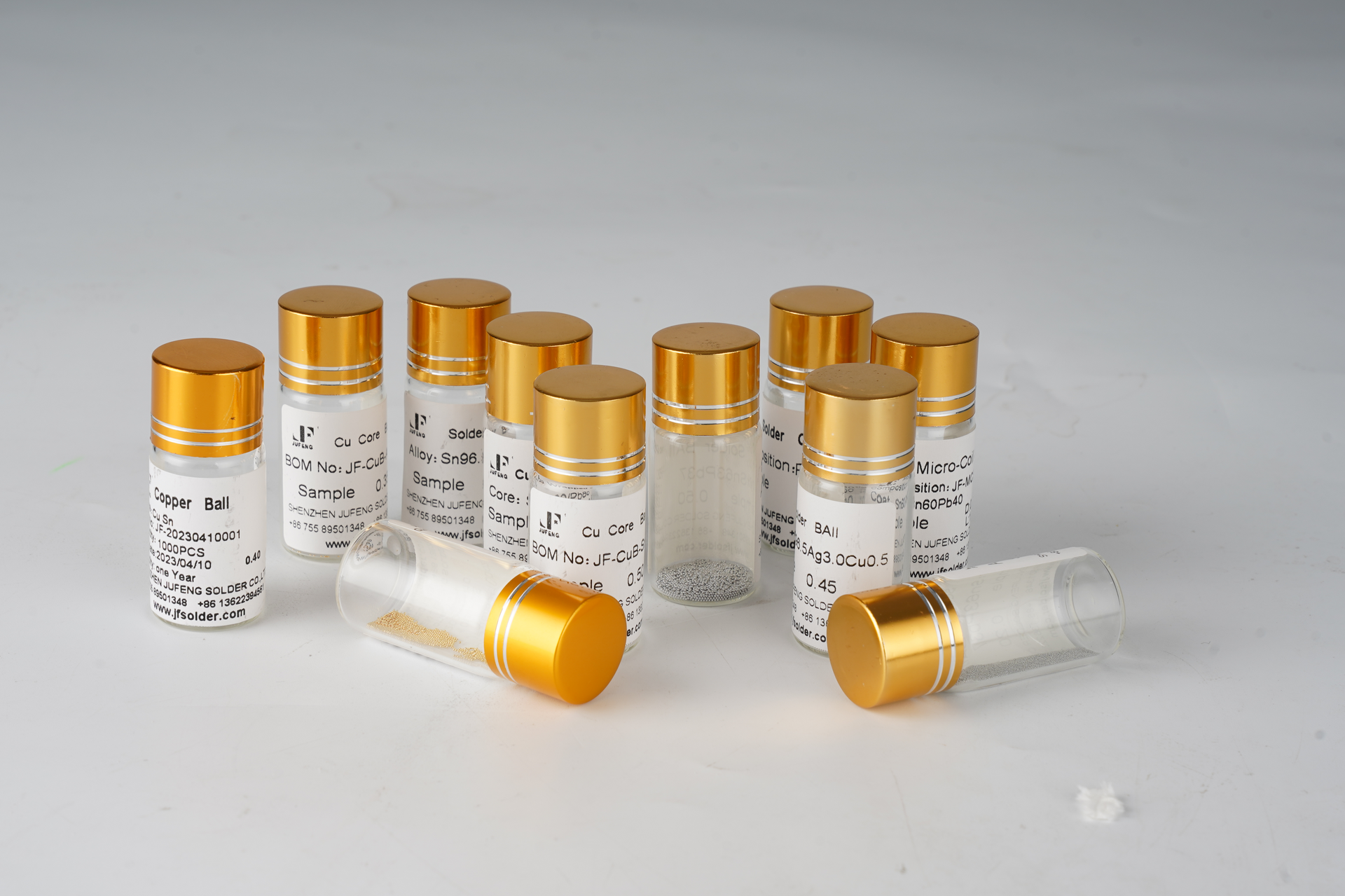
Copper Cored Ball
JuFeng
Copper Cored Ball
JuFeng
- Excellent BLT control, capable of constructing high-reliability and ultra-fine pitch 3D packaging structures
- High conductivity, high heat dissipation, and good electromigration resistance
- Provide solder alloy-coated copper core balls and gold-plated copper core balls
Solder Sphere
JuFeng
Solder Sphere
JuFeng
- Uniform sphericity and small diameter tolerance
- Excellent oxidation resistance, high solderability, and high reliability
- Available in 0.05mm - 1.0mm and customized sizes
Optical Edge Profile Inspection Tool
Delta Electronics
Optical Edge Profile Inspection Tool
Delta Electronics
- Helps identify problems in advance and take appropriate measures to reduce defect rates
- Automated inspection functions enable automatic detection and analysis, reducing manual operation
- Improves inspection efficiency and consistency
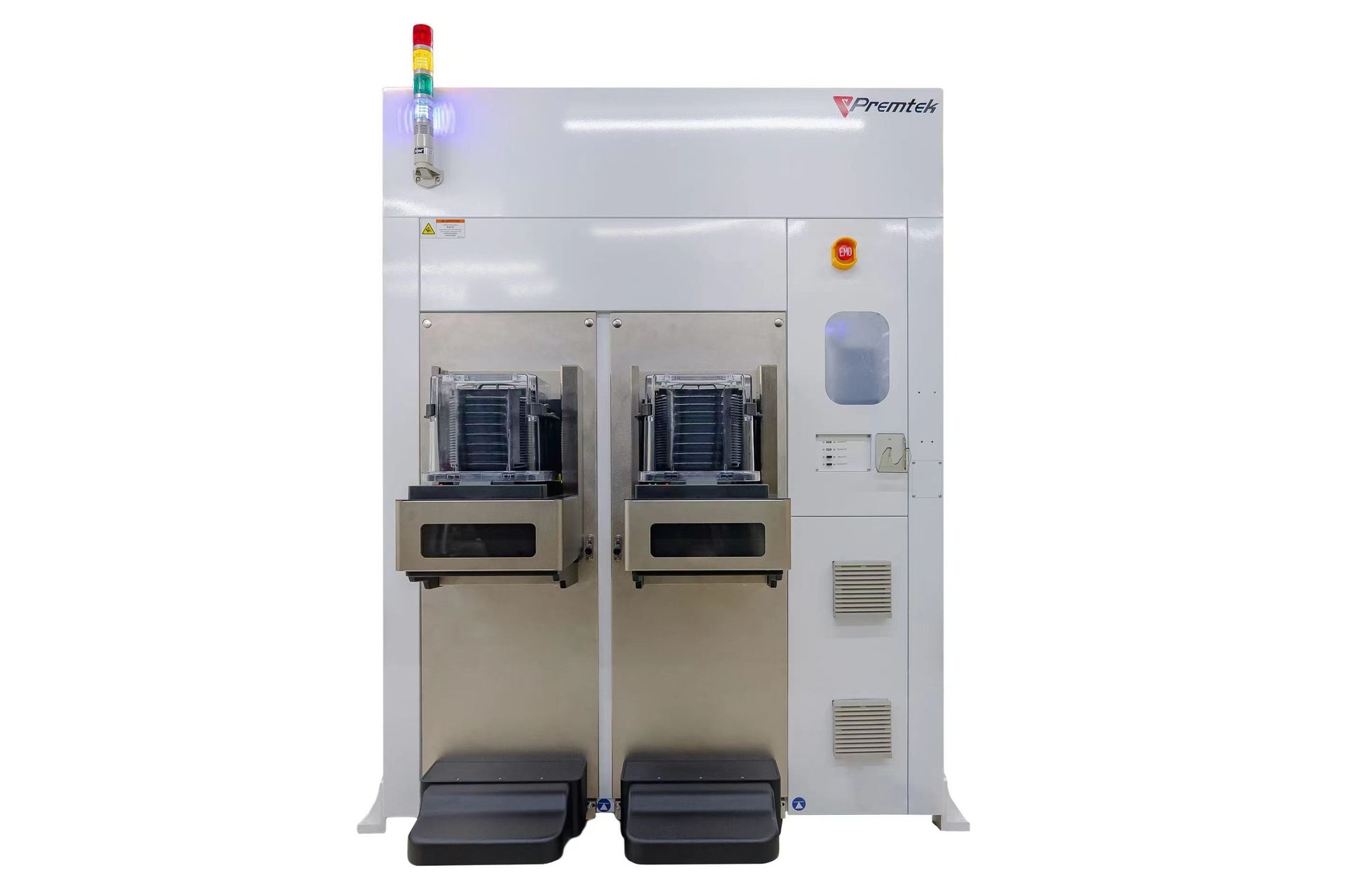
Rapid Thermal Processing
Premtek
Rapid Thermal Processing
Premtek
- Supports both 8” & 6” wafer production
- Configurable SMIF / Open cassette load port
- Compatible with both atmospheric / Vacuum process, Oxygen-free processing with O2 < 1 ppm
- SECS / GEM communication ready, Compliant with SEMI-S2/CE standards
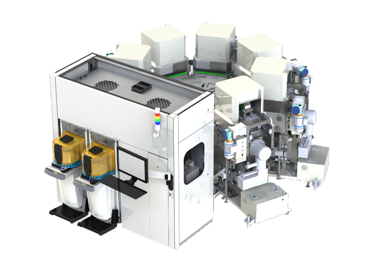
PVD
Skytech
PVD
Skytech
- Can choose cavity configuration according to needs, highly customized, up to a maximum of 6 cavities
- Optional thin film processing architecture, ICP, degas, or long throw architecture
- Reactive sputtering can be optionally combined with in-situ pasting modules
- Highly automated with SECS/GEM
PVD Carbon
Skytech
PVD Carbon
Skytech
- Coating using high-vacuum physical methods
- Carbon film has high purity, high density, and few impurities
- Provide a good stair step coverage effect
- Special design to reduce particles
ALD
Skytech
ALD
Skytech
- High degree of customization and automation
- In response to high and low temperatures and charge damage concerns, Thermal ALD or PEALD can be chosen
- Patented intake design and showerhead system design for excellent uniformity
- Commonly used in processes such as Al2O3, SiO2, AlN, ZrO2, SiNX, HfO2, TiN, TiO2, and metal Mo
Temporary Bonding & De-Bonding
Skytech
Temporary Bonding & De-Bonding
Skytech
- Alignment accuracy less than ± 50um
- Specialized bubble-free construction method
- Can bond 150/150mm with the same size
- Suitable for applications in GaAs, GaN, SiC, LED, 3DIC, and other fields
Descum/Plasma Polish
Skytech
Descum/Plasma Polish
Skytech
- After developing with photoresist or PI, desicum can be used to remove the residue of PR or PI
- Removal of Laser Release Layer
- Dry etching is applicable to ABF
- Suitable for removing the damaged layer using plasma polishing after grinding SiC chips
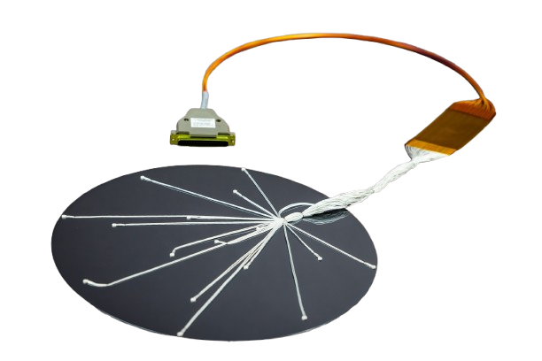
TC Wafer Surface Temperature Sensor
Premtek
TC Wafer Surface Temperature Sensor
Premtek
- Correspond to wafers of various sizes and substrates of different materials
- Temperature range: -200 ℃~1200 ℃
- The number of sensors can be customized according to demand
- High specification accuracy: sensor to sensor ± 0.5°
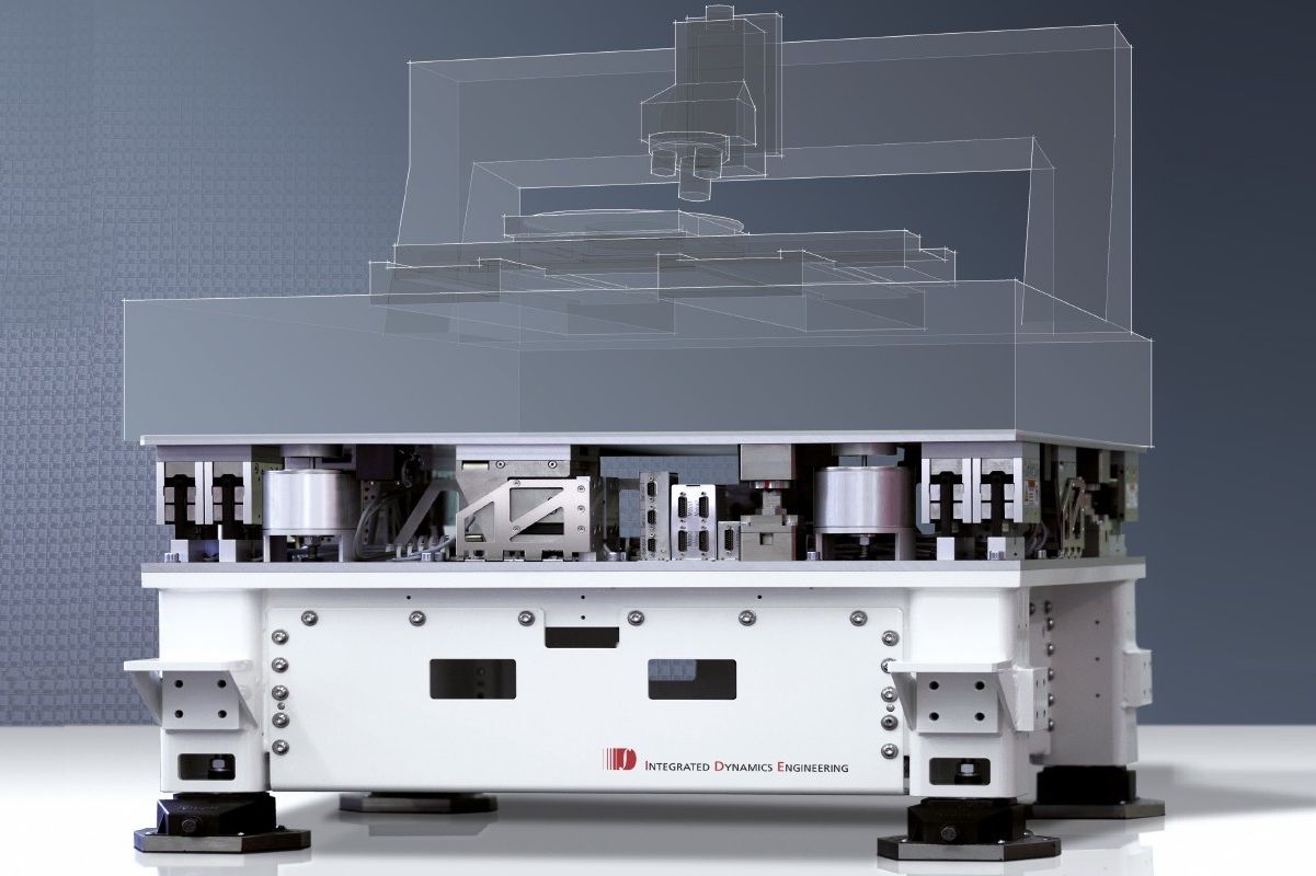
Active/Passive Vibration Isolation Systems
IDE
Active/Passive Vibration Isolation Systems
IDE
- Provides 40 dB isolation at 5 Hz and 60 dB isolation at 20 Hz
- Based on different environmental conditions and equipment vibration isolation requirements, computer simulations are used to offer customers various models and configurations
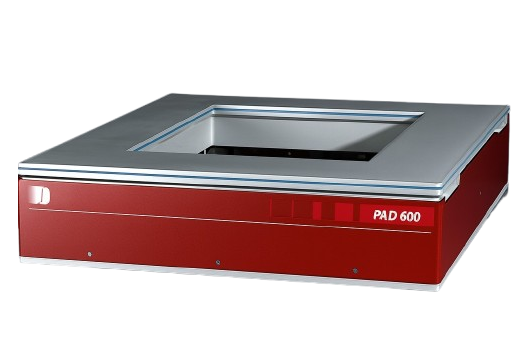
High-Frequency and Low-Frequency Vibration Isolation Tables for Electron Microscopes
IDE
High-Frequency and Low-Frequency Vibration Isolation Tables for Electron Microscopes
IDE
- A unique solution specifically designed for nanotechnology laboratory applications of electron microscopes
- Featuring a distinctive floor feed-forward technology that delivers outstanding vibration isolation even below 1 Hz
- Provides the most effective isolation against high-amplitude disturbances
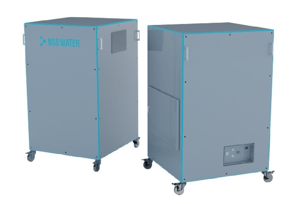
Sustainable Water Treatment Solutions for Advanced Semiconductor Processes
NSS Water
Sustainable Water Treatment Solutions for Advanced Semiconductor Processes
NSS Water
- WET technology can reduce water consumption by up to 90%, thanks to its point-of-use process and ultra-high water purity
- WET’s simplified process (eliminating the need for reverse osmosis and filtration) can reduce energy consumption per liter of water by up to 50%
- Reduces water usage and enables reuse: Wet can serve as a point-of-use recovery system, returning water directly to the production process or discharging it to the wastewater treatment plant
Epoxy Resin Solutions
SEKISUI
Epoxy Resin Solutions
SEKISUI
- Reduced KOZ (Keep-Out Zone)
- Simplified process (no need for flux removal or underfill)
- Excellent solder joint reliability
Formic Acid Reflow Equipment
LEBOSEMI
Formic Acid Reflow Equipment
LEBOSEMI
- Using formic acid reflow technology, eliminating the need for flux coating and cleaning
- Simple process, low cost, and effective in increasing productivity
- Applicable to 6-inch, 8-inch, and 12-inch standard as well as warped wafers
Water Jet Guided Wafer Dicing Tool
SUGINO
Water Jet Guided Wafer Dicing Tool
SUGINO
- Minimal heat-affected zone with high-precision microfabrication, suppressing microcracks and supporting processing down to φ0.1 mm
- Arbitrary shapes with straight cutting, not limited by focal depth, ensuring no edge inclination
- Compatible with various materials, enabling the processing of both semiconductors and high-hardness materials
Equipment Foundation with Active/Passive Vibration Isolation System
Ho Guang Machinery
Equipment Foundation with Active/Passive Vibration Isolation System
Ho Guang Machinery
- Design and Manufacturing of Anti-Vibration Steel Structures and Vibration Isolation Engineering
- Rigid Vibration-Isolated Equipment Base
High-Pressure Annealing and High-Pressure Oxidation Furnace
YEST
High-Pressure Annealing and High-Pressure Oxidation Furnace
YEST
- Improved film quality: reduces oxygen vacancies and defect density, enhancing dielectric reliability (TDDB, BTI)
- Excellent uniformity: under high pressure, the higher reactivity of oxygen or nitrogen ensures both wafer-to-wafer and within-wafer uniformity
- Wide applicability: suitable for SiO₂/SiON gate oxides, high-k dielectrics (e.g., HfO₂, Al₂O₃), as well as metal electrode interface repair
PI/PBI Curing and Wafer Baking Furnace
YEST
PI/PBI Curing and Wafer Baking Furnace
YEST
- PI/PBI curing furnace tubes for advanced semiconductor packaging
- Wafer baking furnace tubes for simulating harsh environments
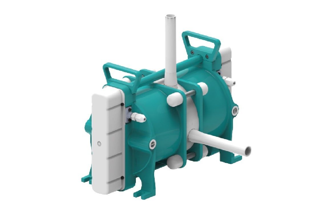
Bellows Pumps for Wet Process and CMP Equipment
LOT CES
Bellows Pumps for Wet Process and CMP Equipment
LOT CES
- Precision and stable bellows pumps with proven experience in high-volume manufacturing (HVM) at semiconductor fabs
- Compared with other suppliers, we offer shorter lead times and more competitive pricing
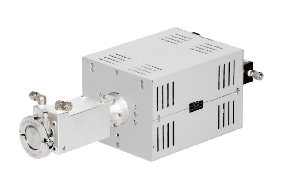
Dry Pump Pre-treatment Plasma System and Dry Pump Remote Plasma System
LOT CES
Dry Pump Pre-treatment Plasma System and Dry Pump Remote Plasma System
LOT CES
- Extend the mean time between failures (MTBF) and service life of dry vacuum pumps
- Proven experience in high-volume manufacturing (HVM) at semiconductor fabs
Dry Pumps
LOT Vacuum
Dry Pumps
LOT Vacuum
- Process-oriented: models available for diffusion, CVD, dry etching, PVD, and other processes
- Predictive system for pump failures
- Ultra-energy efficient with exceptionally long mean time between failures (MTBF)
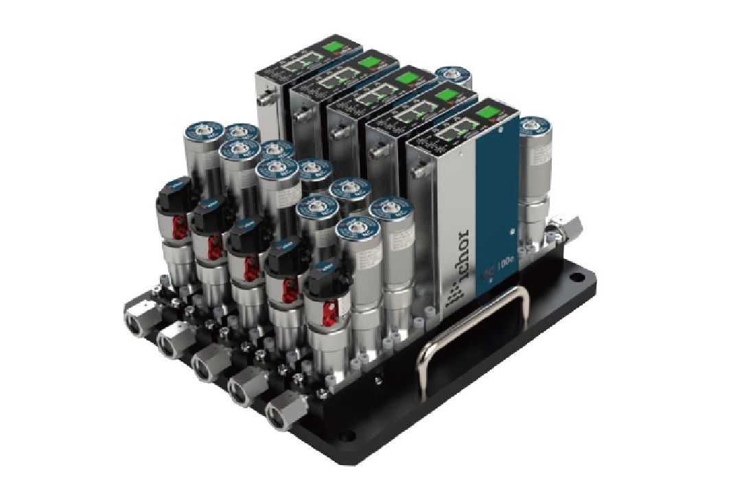
Gas Delivery Subsystems
Ichor
Gas Delivery Subsystems
Ichor
- Highly integrated design, reducing space requirements
- Applied in advanced 7nm/5nm/3nm/2nm diffusion, chemical vapor deposition (CVD), and dry etching equipment
- Providing customized products and services for equipment manufacturers
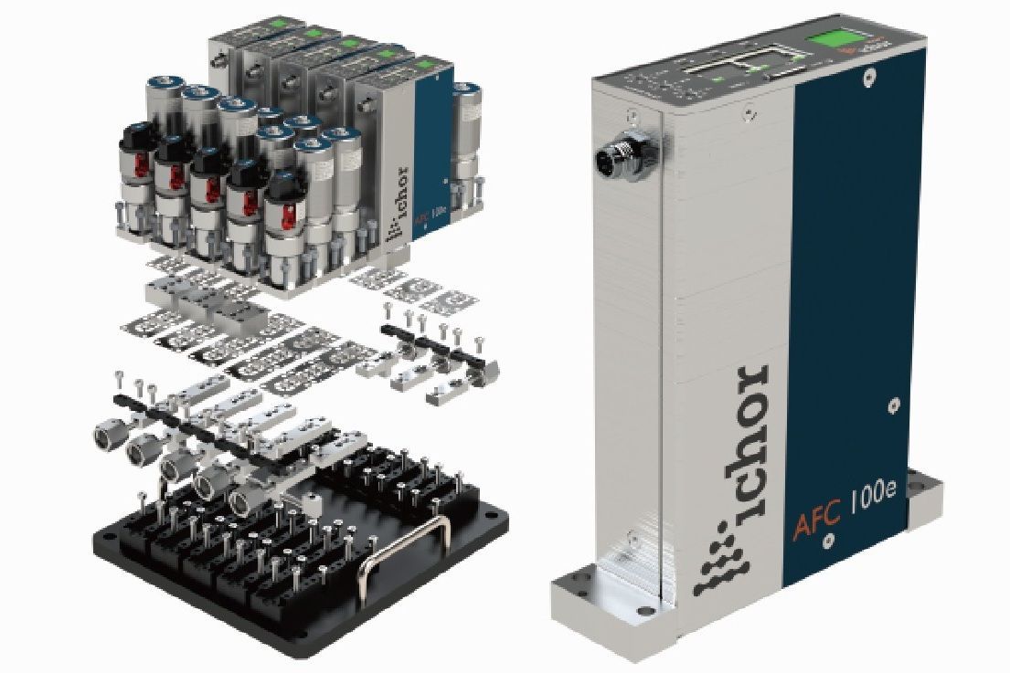
Ultra-Precision Mass Flow Controllers
Ichor
Ultra-Precision Mass Flow Controllers
Ichor
- Applied in advanced 7nm/5nm/3nm/2nm diffusion, chemical vapor deposition (CVD), and dry etching equipment
- Providing ultra-precise gas mass flow control for the semiconductor industry (AFC/AFCe: setpoint error within 1%)
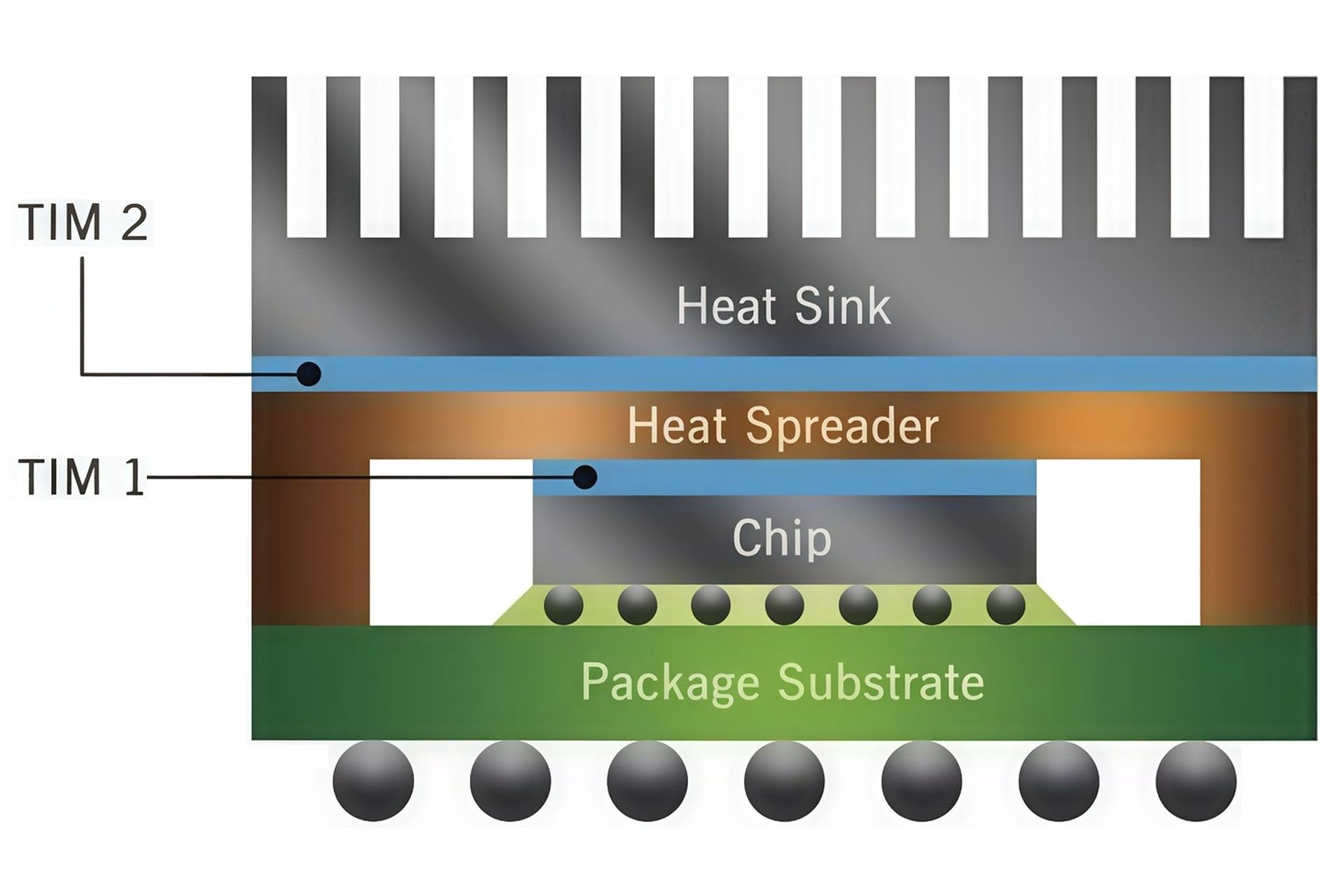
TIM1 (Thermal Interface Material) and Other Materials
ample
TIM1 (Thermal Interface Material) and Other Materials
ample
TIM1 thermal paste and various materials for advanced packaging of AI and HPC chips
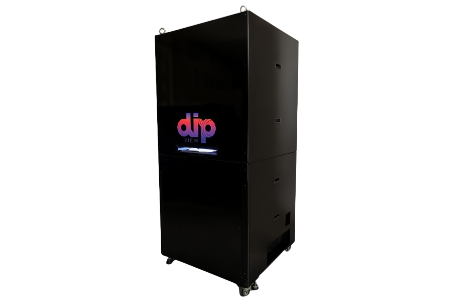
2D/3D Optical Surface Measurement Tool
DIP-View
2D/3D Optical Surface Measurement Tool
DIP-View
- 2D and 3D measurement of roughness, warpage, and shape
- 2D and 3D surface defect measurement
- Thin film stress measurement

Various Components for Electrical Control Boxes of Semiconductor Equipment and SEMI F47 Power Supplies
Phoenix Contact
Various Components for Electrical Control Boxes of Semiconductor Equipment and SEMI F47 Power Supplies
Phoenix Contact
- Providing stable electrical control box components—including terminal blocks, industrial connectors, automation controllers, power modules, and communication interfaces—ideal for semiconductor equipment applications
- Offering customized products and services for equipment manufacturers
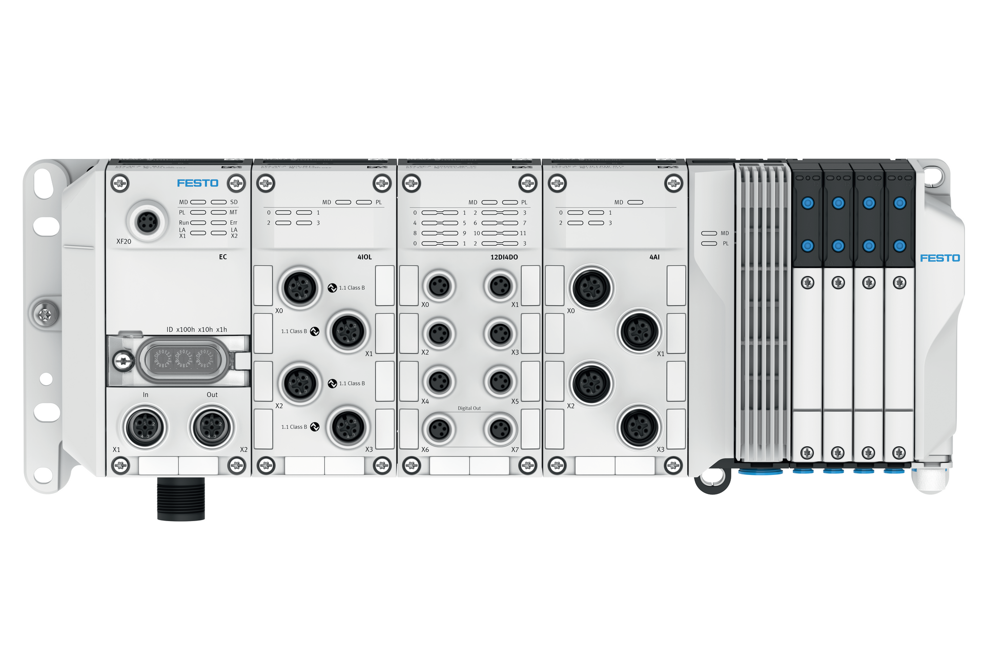
Micro-Contamination Control Solutions with MFCs, Flow Meters, and More for N₂ Purgers and Air Curtain Systems
FESTO
Micro-Contamination Control Solutions with MFCs, Flow Meters, and More for N₂ Purgers and Air Curtain Systems
FESTO
- Proven experience in high-volume manufacturing (HVM) at semiconductor fabs
- Compared with other suppliers, we offer shorter lead times and competitive pricing
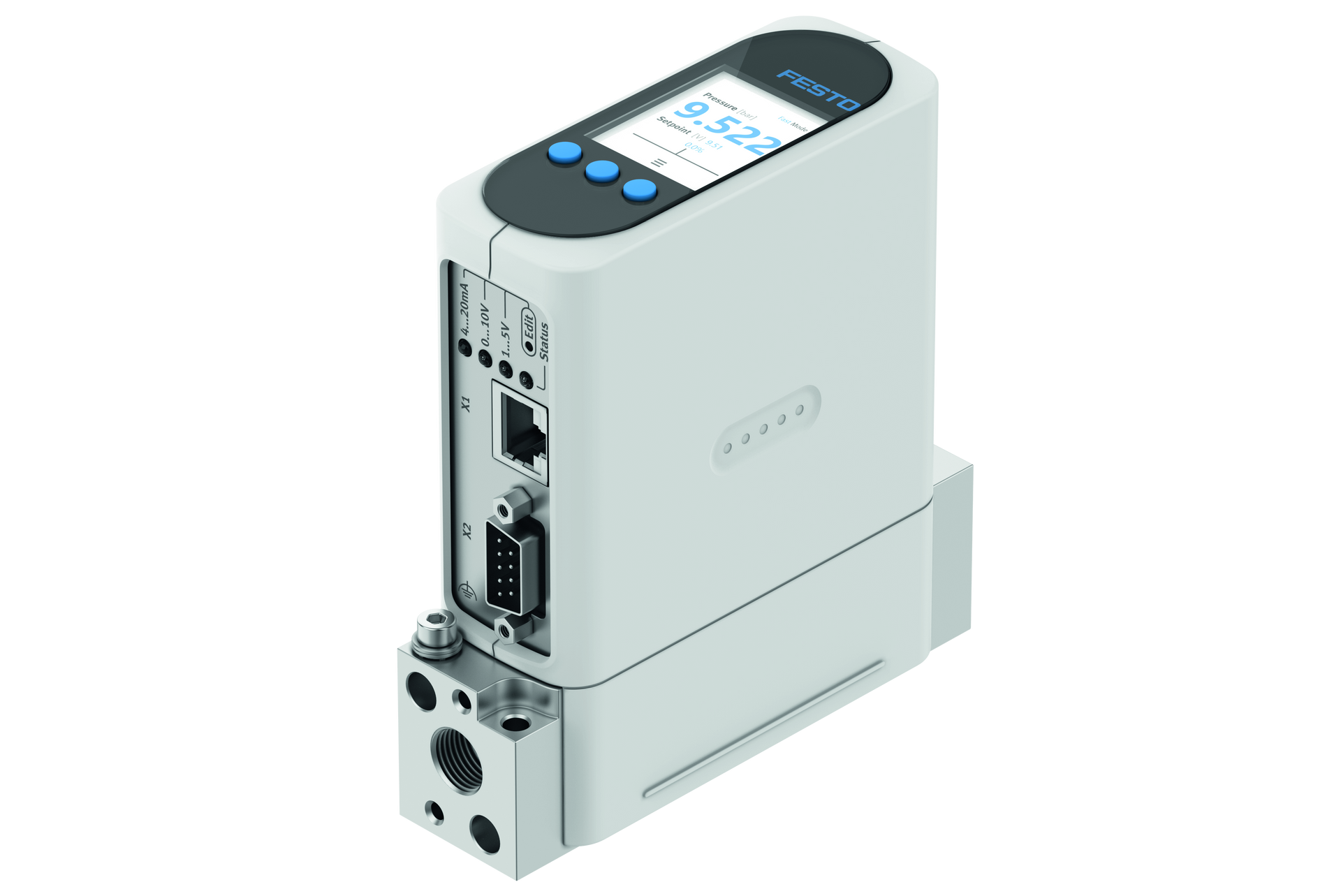
Pneumatic Control Components and Modules
FESTO
Pneumatic Control Components and Modules
FESTO
- Pneumatic components for semiconductor equipment, such as cylinders, solenoid valves, fittings and tubing, and air preparation units
- Precise and stable, with proven experience in high-volume manufacturing (HVM) at semiconductor fabs
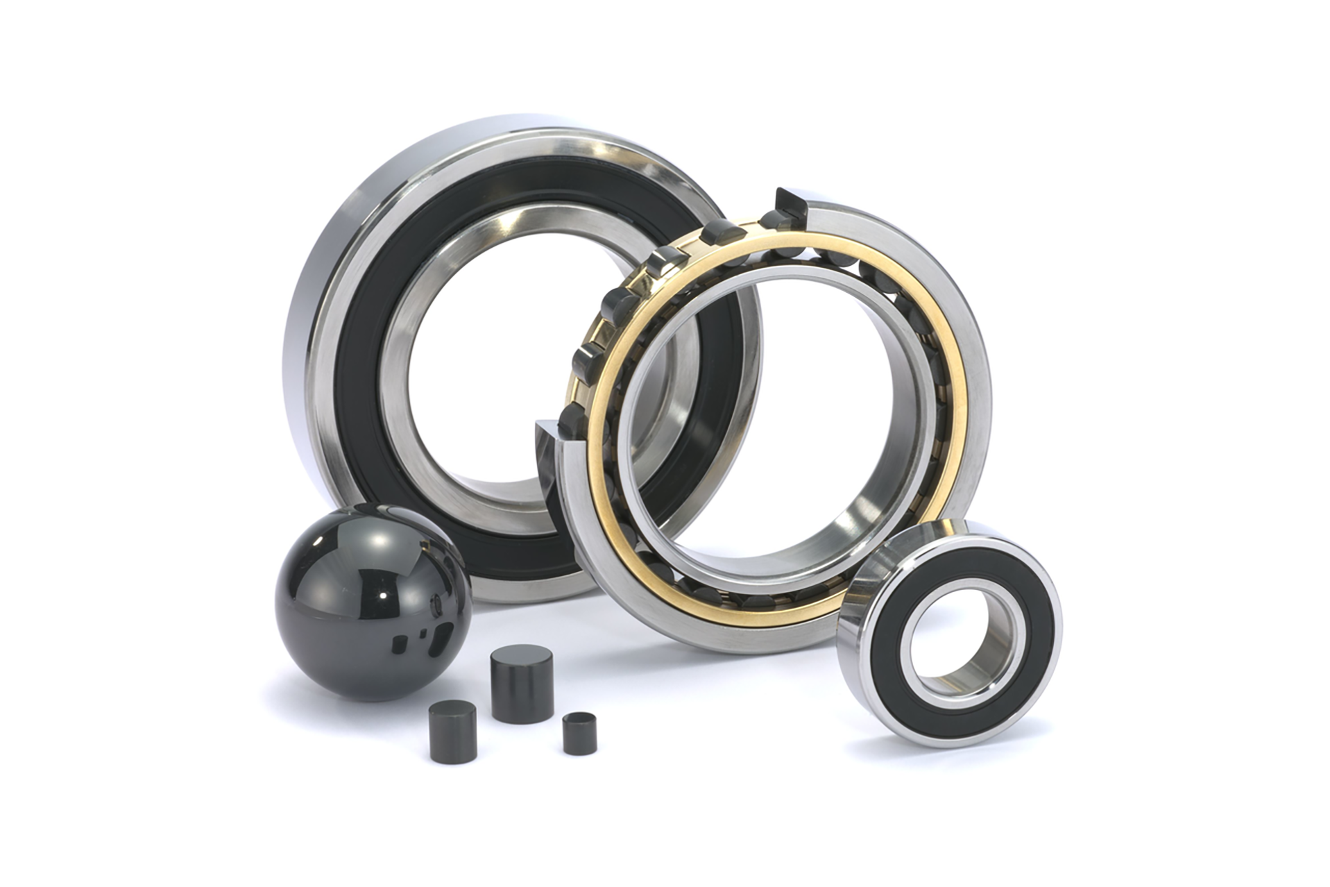
Precision Metal/Ceramic Bearings and Spindles
SKF
Precision Metal/Ceramic Bearings and Spindles
SKF
- Various metal and ceramic bearings for semiconductor equipment
- Spindles for semiconductor wafer grinding, polishing, and photoresist coating equipment, as well as cleanroom environmental monitoring solutions
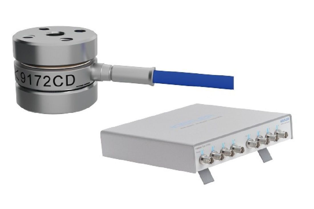
Piezoelectric Sensing Components
KISTLER
Piezoelectric Sensing Components
KISTLER
- Force and Pressure Sensors
- Accelerometers and Vibration Monitoring
DC Power Supplies, RF Generators, and RF Matching Networks
Seiki
DC Power Supplies, RF Generators, and RF Matching Networks
Seiki
- Primarily used in semiconductor thin film, dry etching, and related equipment
- DC Power Supply: high stability, arc suppression, and precise voltage/current control
- RF Generator: fast matching, wide frequency range, low reflection, and stable power output

Ultra-High Precision Printing Equipment for Advanced Packaging and Micro LED
Hummink
Ultra-High Precision Printing Equipment for Advanced Packaging and Micro LED
Hummink
- Proprietary high-precision technology derived from AFM, enabling sub-micron line printing
- Compatible with conductive or insulating inks and adhesives, applicable to advanced packaging as well as specialized circuit fabrication and repair
FOUP Clean
Kromax
FOUP Clean
Kromax
- High-efficiency particle removal to minimize contamination risks
- Designed to meet stringent cleanliness requirements for advanced semiconductor processes
- Reduces cross-contamination and improves overall yield performance
- Ensures consistent and reliable FOUP cleaning performance
- Enhances wafer handling stability and overall process reliability
UV Tape
SEKISUI
UV Tape
SEKISUI
- High heat and chemical resistance for demanding processes
- Easy, damage-free debonding to improve yield
- Low-residue design to reduce cleaning effort